Optoelectronic integrated circuits (OEIC) have attracted the interest of many researchers because of their important role in the hardware for information technology. The optical receivers have key roles in high-speed optical fiber communications, in high-speed chip-to-chip interconnections in computers, efficient networking between computers and in other diverse areas such as medical imaging. One of the most critical building blocks in an optical link system is the transimpedance amplifier (TIA), which converts the photodiode (PD) current into an amplified voltage. The requirements for a typical TIA are high bandwidth, high transimpedance gain, adequate power gain, low noise, low input impedance, small area and low power consumption for array applications.1-4
The major design goals of the TIAs are the transimpedance gain and equivalent input noise current density. The transimpedance gain of the TIAs must be large enough to overcome the noise of the subsequent stage, typically a 50 Ω driver or a limiting amplifier. The equivalent input noise current density determines the minimum input current that yields a given bit error rate, directly impacting the link budget. Unfortunately, the transimpedance gain and equivalent input noise current density cannot be measured directly from microwave and noise equipment, while the S-parameters and noise figure of the TIAs can be measured with a vector network analyzer (VNA) and a noise figure meter in a straightforward manner. Therefore, a fast transformation between S-parameters/noise figure and transimpedance gain/equivalent input noise current density is needed.
Analytical expressions for trans-impedance gain and equivalent input noise current of optical receivers have been derived5 and simple expressions for the relationship between the transimpedance gain and Z-parameters are given.6-8 However, these expressions are not always valid and the transimpedance gain and equivalent input noise current density cannot be directly and accurately calculated from S-parameters and noise figure measurement data. Based on the author’s knowledge, a comprehensive analysis for fast transformation between S-parameters/noise figure and transimpedance gain/equivalent input noise current density has not yet been published.
In this article, a simple but efficient transformation technique for TIAs is proposed and the analytical expressions for the relationships between the transimpedance gain and S-parameters, the equivalent input noise current density and the noise figure for high-speed optical transimpedance preamplifier design are derived. This technique is based on the signal and noise equivalent circuit model of the optical receiver front-end.
In contrast with previous publications,5-8 this method has the following advantages:
- The transimpedance gain can be directly derived from S-parameters for arbitrary source and load impedances and simplified expressions for two special cases (source impedances are zero and 50 Ω) are also given.
- The equivalent input noise current density can be determined from noise figure measurements without four noise parameters (minimum noise figure, noise resistance and optimum source reflection coefficient) of TIA in 50 Ω and non-50 Ω systems.

Figure 1 Simulated model of the optical receiver front-end.
Theoretical Analysis
Transimpedance Gain
The schematic of the optical receiver front-end circuit is shown in Figure 1, where YS is the photodiode (PD) input admittance. Typically this will be that of the PIN/APD and it is almost totally capacitive (that is YS = jωCpd). YL is the load admittance, which is generated by the input admittance of the next stage (typically YL = Y0 = 0.02 mS).
The transimpedance is defined as the magnitude of the ratio of the output voltage V2 at a load impedance and the photocurrent through the photodiode is. Based on the small-signal circuit model analysis for an optical receiver frond-end and applying Kirchhoff’s current law, the transimpedance gain of the optical receiver front-end can be expressed as:

The relationship between the S-parameters and Y-parameters can be expressed as:
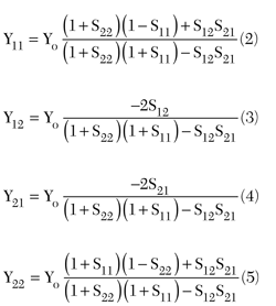
where Y0 ( = 0.02 mS) is the characteristic admittance of the system.
Substituting Equations 2 to 5 into Equation 1:
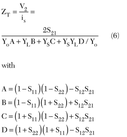
If the source impedance is infinite (that is YS = 0), and the output end of the TIA is connected to a matched load (that is YL = Y0 = 0.02 mS), the corresponding transimpedance gain of the receiver front-end can be simplified as follows:

when the TIA is operated in a 50 Ω system (YL = YS = Y0 = 20 mS), the transimpedance gain can be written as:


The transimpedance gain and bandwidth versus YS and YL are summarized in Table 1. It can be observed that the transimpedance 3 dB bandwidth can be determined from the forward transmission coefficient S21 only when the input and output ports are terminated in matched loads. The physical meanings of the three transimpedance gains mentioned above are as follows: ZT is the transimpedance gain of whole optical receiver front-end (PD+TIA);  is the transimpedance gain of TIA; and
  is proportional to the power gain S21 of the TIA.

Figure 2 Noise model of the 50 Ω noise figure measurement system for an optical preamplifier.
Equivalent Input Noise Current Density of the TIA
Figure 2 shows the noise model of the noise figure measurement system for an optical preamplifier. It is noted that 50 Ω standard resistances have been used for source and load impedances (ZS=ZL=Z0=50 Ω).  and
and  are the input and output impedances of the TIA, respectively.
  is the total output noise voltage density, and
  is the equivalent input noise current density of the TIA.
The noise figure of the TIA can be expressed as follows:10

Where Av is the voltage gain and can be expressed as:

Where  is the transimpedance of the TIA
  . The corresponding equivalent input noise current density of the TIA
  can be derived as follows:


Figure 3 Noise model of the optical receiver front-end.
Equivalent Input Noise Current Density of the Optical Receiver Front-end
Figure 3 shows the noise model of a typical optical receiver front-end in a non-50 Ω system, where  is the total equivalent input noise current density and
  is the total output noise voltage density of the receiver front-end. It is noted that the input port of the TIA is connected to the PD, not the matched load. Therefore, Equation 13 is only valid for TIA design, not for the whole receiver front-end.
Assuming that the total output noise voltage density  is generated mainly by the TIA (here the noise contribution of the PD is neglected), the equivalent input noise current density of the receiver front-end
  can be expressed as follows:

Traditionally, the output end of TIA is connected to a matched load (Yl =Yo=0.02 mS), then  can be written as:

when the TIA is operated in a 50 Ω system (YL = YS = Y0 = 20 mS), the equivalent input noise current density can be simplified:


It is noted that Equation 16 is the conventional formula for predicting the equivalent input noise current density for a TIA IC. The  is dependent on the noise figure only, and independent on the S-parameters of the TIA. The equivalent input noise current density versus YS and YL is summarized in Table 2.
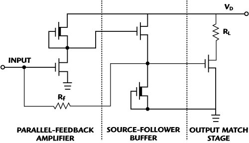
Figure 4 Schematic of the 10 Gb/s HEMT-based TIA IC.
Experimental Analysis
In order to demonstrate the expressions derived in the Theoretical Analysis section for the TIA, a HEMT-based TIA, which operates at 10 Gb/s, has been designed using a 0.2 µm PHEMT process.11 Figure 4 shows a schematic of the developed TIA IC, using both enhancement- and depletion-mode (E-D) transistors. This IC consists of three parts: a parallel-feedback amplifier core, a source-follower buffer and an output match stage. The source-follower buffer improves the flatness of the gain-frequency characteristics by separating the parallel-feedback loop from the large input capacitance of the output buffer (that is eliminating the Miller capacitance loading to the previous stages). The output stage is designed for a 50 Ω output impedance match. Figure 5 shows the experimental setup. All measurements were carried out on-wafer, using Air-Coplanar Probes. The wafer probes were calibrated using the Line-Reflect-Match (LRM) calibration method for S-parameter measurement. The noise parameter measurement method proposed here has been tested on wafer up to 26 GHz. The corresponding chip photograph of the 10 Gb/s HEMT TIA is shown in Figure 6.11
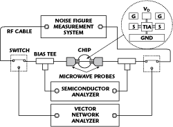
Figure 5 Experimental setup.

Figure 6 Photograph of the 10 Gb/s HEMT TIA chip.
Figure 7 shows the measured magnitudes and phases of the S-parameters of the TIA IC. The high gain |S21| of 25 dB and the broad 3 dB bandwidth over 10.8 GHz have been obtained. Good matching is also achieved, |S11| less than -10 dB and |S22| less than -7 dB for the whole frequency range. The corresponding noise figure versus frequency is shown in Figure 8.
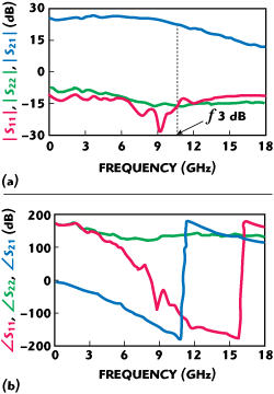
Figure 7 S-parameters of the 10 Gb/s HEMT-based TIA IC: (a) magnitude and (b) phase.

Figure 8 Measured noise figure of the 10 Gb/s HEMT-based TIA IC.
The transimpedance gain (TG) and equivalent input noise current density (EINCD) can be obtained from AC and noise signal analysis by using commercial circuit design tools (such as SPICE). However, it is difficult to measure them directly using conventional microwave signal and noise measurement systems. Alternatively, they can be calculated from S-parameters and noise figure measurements by using the proposed transformation expressions.

Figure 9 Transimpedance gain vs. frequency for the 10 Gb/s TIA.

Figure 10 3 dB bandwidth of the transimpedance gain vs. capacitance of PD.
Figure 9 shows the transimpedance gain, which is derived from the measured S-parameters of the 10 Gb/s TIA; the corresponding 3 dB bandwidth versus capacitance of the PD is shown in Figure 10. It can be found that the 3 dB bandwidth of the TIA transimpedance gain is approximately 11.5 GHz, and the corresponding optical receiver front-end 3 dB bandwidth decreases with the increase of the capacitance of the PD (YS = jωCpd). As long as the capacitance of the PD is kept less than 0.6 pF (3 dB bandwidth of 8 GHz), the proposed TIA can be operated at a 10 Gb/s bit rate. Figure 11 shows the comparison of the predicted transimpedance gain for the 10 Gb/s TIA obtained from Equations 7 and 8. It is obvious that the gain and bandwidth predicted by Equation 7 is better than that of a TIA operating in a matching system. That means the transimpedance gain will be underestimated using the conventional formula.

Figure 11 Comparison of transimpedance gains for 10 Gb/s TIA.
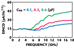
Figure 12 Equivalent input noise current density. (EINCD) vs. frequency for the 10 Gb/s TIA
Figure 12 shows the EINCD, which is derived from the measured noise figure of 10 Gb/s TIA. The corresponding average values versus capacitance of the PD are shown in Figure 13. It can be found that equivalent input noise current density increases with the increase of capacitance of the PD (YS = jωCpd). As long as the capacitance of the PD is kept less than 0.3 pF, the equivalent input noise current density of the proposed TIA can be less than  Figure 14 shows the comparison of predicted equivalent input noise current density for the 10 Gb/s TIA by using the proposed Equation 13 and the conventional Equation 16. It is obvious that the equivalent input noise current density predicted by Equation 13 is better than that predicted by the conventional formula. This means the equivalent input noise current density will be overestimated using the conventional formula.

Figure 13 Equivalent input noise current density (EINCD) vs. capacitance of PD.
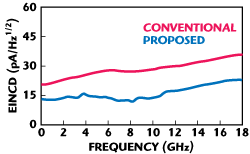
Figure 14 Comparison of the equivalent input noise current density (EINCD) for the 10 Gb/s TIA.
Conclusion
Analytical expressions for the relationships between the transimpedance gain from S-parameters, equivalent input noise current density and noise figure for high-speed optical transimpedance preamplifier design is proposed in this article. The validity of the new approach is proven by using a 10 Gb/s high electron mobility transistor (HEMT)-based transimpedance preamplifier.
References
- S. Kimura and Y. Imai, “0 to 40 GHz GaAs MESFET Distributed Baseband Amplifier ICs for High-speed Optical Transmission,” IEEE Transactions on Microwave Theory and Techniques, Vol. 44, No. 11, November 1996, pp. 2076-2082.
- J.S. Weiner, J.S. Lee and A. Leven, et al., “An InGaAs-InP HBT Differential Transimpedance Amplifier with 47 GHz Bandwidth,” IEEE Journal of Solid-State Circuits, Vol. 39, No. 10, October 2004, pp. 1720-1723.
- J. Gao, B. Gao and C. Liang, “PIN PD Microwave Equivalent Circuit Model for Optical Receiver Design,” Microwave and Optical Technology Letters, Vol. 38, No. 2, pp. 102-104.
- C. Kromer, G. Sialm, T. Morf, M.L. Schmatz, F. Ellinger, D. Erni and H. Jackel, “A Low-power 20 GHz 52 dB Transimpedance Amplifier in 80 nm CMOS,” IEEE Journal of Solid-State Circuits, Vol. 39, No. 6, June 2004, pp. 885-894.
- A. Leven, R. Reuter and Y. Baeyens, “Unified Analytical Expressions for Transimpedance and Equivalent Input Noise Current of Optical Receivers,” IEEE Transactions on Microwave Theory and Techniques, Vol. 48, No. 10, October 2000, pp. 1701-1706.
- Y. Suzuki and K. Honjo, “Wideband Transimpedance Amplifiers Using AlGaAs/InxGa1-xAs Pseudomorphic 2-D EG FETs,” IEEE Journal of Solid-State Circuits, Vol. 33, No. 10, October 1998, pp. 1559-1562.
- J.S. Weiner, A. Leven, V. Houtsma, Y. Baeyens, Y.K. Chen, P. Paschke, Y. Yang, J. Frackoviak, W. J. Sun, A. Tate, R. Reyes, R.E. Kopf and N.G. Weimann, “SiGe Differential Transimpedance Amplifier with 50 GHz Bandwidth,” IEEE Journal of Solid-State Circuits, Vol. 38, No. 9, September 2003, pp. 1512-1517.
- M.B. Das, J.W. Chen and E. John, “Designing Optoelectronic Integrated Circuit (OEIC) Receivers for High Sensitivity and Maximally Flat Frequency Response,” IEEE Journal of Lightwave Technology, Vol. 13, No. 9, September 1995, pp. 1876-1884.
- J. Ortiz and C. Denig, “Noise Figure Analysis Using SPICE,” Microwave Journal, Vol. 35, No. 4, April 1992, pp. 89-94.
- J. Gao, RF and Microwave Modeling and Measurement Techniques for Field Effect Transistors, SciTech, USA, 2009.
- S. Cai, Z. Wang, J. Gao and E. Zhu, “Analysis and Design of 10 Gb/s 0.2 m PHEMT Transimpedance Amplifier,” Chinese Journal of Semiconductor, Vol. 27, No. 10, October 2006, pp. 1809-1813.
Jianjun Gao received his BEng and PhD degrees from Tsinghua University in 1991 and 1999, respectively, and his MEng degree from the Hebei Semiconductor Research Institute in 1994. From 1999 to 2001, he was a post-doctoral research fellow at the Microelectronics R&D Center, Chinese Academy of Sciences, developing PHEMT optical modulator drivers. In 2001, he joined the school of Electrical and Electronic Engineering, Nanyang Technological University (NTU), Singapore, as a research fellow in semiconductor device modeling and on wafer measurement. In 2003, he joined the Institute for High-Frequency and Semiconductor System Technologies, Berlin University of Technology, Germany, as a research associate working on InP HBT modeling and circuit design for high speed optical communication. In 2004, he joined the Electronics Engineering Department, Carleton University, Canada, as a post-doctoral fellow, working on the semiconductor neural network modeling technique. From 2004 to 2007, he was a full professor in the radio engineering department at Southeast University, Nanjing, China. Since 2007, he has been a full professor in the school of information science and technology, East China Normal University, Shanghai, China. His main areas of research include characterization, modeling and on wafer measurement of microwave semiconductor devices, optoelectronics device and high-speed integrated circuit for radio frequency and optical communication.
