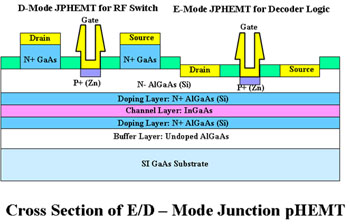
Sony's JPHEMT process has been enabling high performance switches and antenna switch modules (ASM) for quite some time, and they continue to release some of the highest performance MMIC switches and ASMs on the market today especially for handset applications. Their process roadmap shows them developing higher performance switches with new process improvements and are working on power amplifiers that will leverage the same JPHEMT process advantages.
For switches, the JPHEMT process features high linearity, loss insertion loss, low voltage operation, on-chip logic integration and processed on a 6 inch wafer line. For power amplifiers, it features high efficiency and high linearity including integration with switches. logic control and passive circuits. They are developing WiMAX and LTE PAs for release later this year with samples available now for WiMAX. Target performance is PAE=32% at Pout=27dBm for LTE Band7.
 The JPHEMT is unique in that the gate contact is not the normal Schottky contact used by other MMIC manufacturers (typically Ti/Pt/Au metallization) as it has a Zn layer underneath the gate metal (see MMIC cross section to the right). This key difference enables Sony to design high performance MMIC switches (including E-PHEMTs) and amplifiers, and they have achieved the best Ron*Coff product for GaAs switches that we have been able to find. They also have the highest number of switch ports for a GaAs MMIC with SP14T ASMs available, and they are manufacturing SOI switches with new product coming out this year. They have an impressive MMIC roadmap and we hope to cover their new products as they are released.
