Lighting is about illuminating our world for a purpose. Whether it be for identification, recognition, beautification, accentuation, decoration, orientation, safety, security or ambience, the associated quest runs for ever more efficient, longer-lasting and sun-like light sources. Efficiency is reducing the amount of energy required to create certain amounts of light flux (lumen [lm]). Longevity strives to achieve maintenance-free, everlasting lighting systems. Finally, “sun-like” denotes the property of being a “white” light source, one that emits an almost continuous spectrum between 400 and 800 nm wavelengths—just like the sun. This kind of light also guarantees sun-like color rendition: all objects illuminated with a white source appear in their “natural” colors. This is in contrast to a source like the yellow/orange sodium vapor lamp, for example, which on the one hand has a very poor color rendition, but also provides the best currently achievable efficiency (155 lm/W).
The innovative RF lighting source combines several of the above-mentioned properties. It is bright (a small quartz bulb emits easily 10 to 20 klm), sun-like and effective in turning RF energy into light; typically 140 lm/W is achieved. The key technology to deliver the power to drive the RF Light (or Plasma Light) is based on laterally diffused metal oxide semiconductor (Si LDMOS) RF power transistors. These devices are typically used in cellular base stations or broadcast transmitters as final amplifier stages in the frequency range between a few MHz up to 3.8 GHz.1 Recent developments in RF power technology; such as improved ruggedness and strongly enhanced power density up to 1000 W per single transistor device, have enabled their use for RF (plasma) lighting. However, using these transistors as power sources for this new lighting technology poses a few fundamental issues, which are discussed here.
THE NEW RF PLASMA LIGHT SOURCE
Developments in RF power technology, such as improved cost structure, ruggedness and power levels, have enabled a breakthrough light source technology, which is often referred to as ‘RF plasma lighting’. All RF plasma lighting sources make use of a small, electrode-less quartz light bulb, which contains argon gas and metal halide mixtures. The bulb is powered by direct RF radiation, which ignites the gas mixtures to create and power a bright plasma, the color of which can be tuned by the composition of its constituents.
This technology works without any additional electrodes in the bulb, unlike standard high intensity discharge lamps. No electrodes means very long operating lifetimes, since contamination and wire erosion that lead to decreased efficiency and eventual lamp failure are precluded. The RF light source lives up to 50,000 hrs when it reaches 65 to 70 percent of its original light output. Typical high intensity discharge lamps, in comparison, achieve 20,000 hrs operating life. Another strong point of the plasma light is its efficiency: 1 W of RF power is converted to 130 to 140 lm of light.
OTHER TECHNOLOGIES IN COMPARISON
Table 1 summarizes currently available technologies that generate bright light either more or less efficiently. It lists a few key parameters, including lifetime, luminous flux, efficacy, color rendition index, color temperature, start-up time and re-strike time (time to start after switch off from normal operation). Please note that the numbers are only valid for a qualitative comparison.
The plasma light source is among the brightest and most efficient light sources available to date and boasts a very long life time. Important to note is the high brightness per bulb (much brighter than LEDs, for example). Consequently, one needs multiple LEDs to generate the light output of a single plasma light source. Hence, LED luminaries for street lighting will be considerably larger than those for plasma light sources.
Given the high brightness per bulb, the plasma light currently enters the market on the high “output power” end for street lighting and stage lighting, which is true in general for applications requiring more than 5000 lm per luminaire. Competitors in that realm are the incumbent, other metal halide or vapor-based, high intensity discharge lamps and LEDs. On the other hand, light sources like (compact) fluorescents or LEDs serve the < 5000 lm per appliance markets with high efficiency and decreasing color rendition.
RF IMPLICATIONS
In the following, the RF power to drive light sources will be assumed to be generated by Si LDMOS-based transistor devices. The RF-driven Plasma Light is a perfect example for novel applications that can be powered by RF energy in the industrial, scientific, medical (ISM) realm. Established technologies use RF to pump a gas discharge in a laser cavity (such as CO2 and excimer lasers). These “gas discharge” applications and in general most of the ISM applications form highly mismatched RF loads, certainly during some part of the usage cycle. In the case of gas discharges, for instance, the gas cavity acts as “open circuit” during switch-on. This, in turn, means that without protection or other measures, all of the “injected” RF power reflected back into the final stage of the amplifier needs to be dissipated in the transistor(s) right there and most likely will destroy the device(s) if this situation lasts too long. Hence, the final transistors should be extremely rugged to withstand these mismatched situations. After the discharge strikes, the load impedance eventually reverts to “matched” and the transistor sees a good load. Obviously, these mismatched conditions occur every time the plasma is “switched on,” exerting strain on the output devices. The used devices should remain stable and not degrade over time.
As for ruggedness, the efficiency and power handling capability of the devices is important—the more power per surface area, the better. These aspects—ruggedness, efficiency, power (density) and reliability—will now be further discussed for the 28 and 50 V LDMOS processes.
LDMOS TECHNOLOGY
During the last decade, LDMOS technology has evolved2 to become the preferred technology for RF power transistors for many applications. LDMOS transistors are voltage-controlled devices leading to a simple and low cost bias circuitry. Intrinsic properties of LDMOS enable overdrive to +5 dB without risk of failure, high flexibility for different pulse formats and to prevent thermal runaways, making the overall system design much simpler than for incumbent bipolar technologies. Furthermore, the source connection to the bulk-backside of LDMOS allows for the use of environment-friendly ceramic or plastic packages. Nowadays, LDMOS technology operating at 28 V is the leading RF power technology for base station applications, in particular for GSM-EDGE applications at 1 and 2 GHz, W-CDMA applications at 2.2 GHz, and for WiMAX applications at 2.7 and 3.8 GHz. Recently, another LDMOS family member, the 50 V LDMOS,3 has emerged and is used for broadcast, ISM, defense and avionics applications. It combines high power density to achieve power levels up to 600 W per single device4 and outstanding ruggedness with high gain and efficiency at frequencies up to 1.5 GHz.

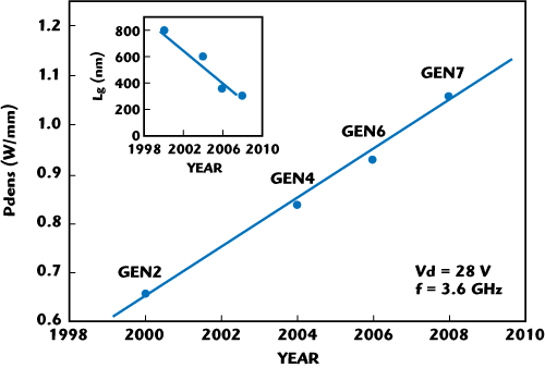
Figure 1 LDMDS evolution of power density at 3.6 GHz.
LDMOS PERFORMANCE EVOLUTION
The improvement in RF performance of LDMOS technology is summarized in Figures 1 and 2 for the 28 V technology at 3.6 GHz, showing the power density and the drain efficiency evolution over the last decade. The power density has doubled, reaching values over 1 W/mm at 3.6 GHz for the latest technologies. The drain efficiency values exceed 50 percent at 3.6 GHz, while efficiency values close to the theoretical Class B efficiency of 78.5 percent are reached for LDMOS at frequencies below 1 GHz.

Figure 2 LDMOS evolution of drain efficiency at 3.6 GHz.
This LDMOS performance evolution has been realized by a continuous reduction of the gate length and of the drain output capacitance5 (see insets of Figures 1 and 2), making use of the capabilities of the high-volume silicon manufacturing processes, with well-known and proven reliability behavior. These properties of high-power density and efficiency make LDMOS the preferred technology for RF lighting applications and opens the path for RF lighting to become a performance and price competitive lighting solution.

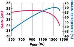
Figure 3 RF class AB performance of a 50 V LDMOS technology device at 225 MHz.
The RF plasma lighting sources can operate over a wide range of RF frequencies, but initial applications typically focus at frequencies of approximately a few hundred megahertz. At these frequencies, both the 28 and 50 V LDMOS technologies can be used, yielding high-efficiency values of 70 to 80 percent and low-heat dissipation, making compact plasma lamp designs possible. The 50 V LDMOS technology has the advantage that the elevated supply voltages lead to higher power densities and higher output impedances for easier matching and more compact designing. Power densities of 2 W/mm can be achieved in combination with high efficiency, as can be seen in Figure 3.6 The drain efficiency at 225 MHz is more than 70 percent for a transistor of 1300 W of (P1dB) pulsed power in combination with a gain of 24 dB. The efficiency can be boosted further towards the 80 to 90 percent by higher harmonic matching. Since the cut-off frequency of LDMOS transistors is above 10 GHz, there is enough power at the higher harmonics to optimize the waveform shapes for high efficiency and change the operation class from AB towards more advanced transistor classes like Class E, F, J,....

Figure 4 Pulsed current voltage measurements of LDMOS for different technologies.
RUGGEDNESS RELIABILITY
These RF lighting applications and most of the ISM applications form highly mismatched RF loads, certainly during some part of the “gas discharge” part of the usage cycle. During this part of the cycle, all of the “injected” RF power is reflected back into the final stage of the amplifier. LDMOS transistors are extremely rugged to withstand these mismatch situations in general and do not degrade over time. Ruggedness, or the ability to withstand “harsh” RF conditions in general, be it mismatch or extremely short pulse rise- and fall-times, is of prime importance to reliable device performance. RF power companies have gone to great lengths to achieve best in class device ruggedness. The technologies have been hardened under the most stringent ruggedness tests during development, which is particularly true for the 50 V technology. Amongst other factors, the base resistance of the parasitic bipolar and the drain extension of the LDMOS device play key roles. These key parameters have been engineered to achieve drain breakdown voltages far exceeding the Class AB supply voltage swing. Drain voltages as high as 150 V for the 50 V technology node can be tolerated, as shown in Figure 4.

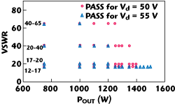
Figure 5 VSWR ruggedness measurements at various output power for a pulsed sign (20% duty cycle) at 225 MHz.
As a ruggedness characterization tool, short pulse (50 to 200 ns) measurements of the current-voltage characteristics are used. The current and voltage are measured with a memory scope during the discharge. The snapback in the I-V curve gives insight in the device properties of the technology. The characterization is done on wafer with small (test) devices in a 50 Ω commercially available setup. Power RF devices cannot be used since the setup is not able to generate enough current. This is a fast and adequate evaluation of device and process changes on ruggedness without influence of test circuits and matching conditions.
These ruggedness tests ultimately result in devices that can withstand VSWRs of at least 10:1 at nominal load, all phase angles and perform flawlessly in the field. The 50 V LDMOS devices can withstand a larger mismatch condition,7 as shown in Figure 5. The device can tolerate 55 V drain voltage in combination with a VSWR of 65:1 at a power of 1 kW, values far above the nominal operation settings for most applications. This extreme ruggedness is of importance for the new “gas discharge” applications, where highly mismatched RF loads—certainly during some part of the usage cycle—can occur.

Figure 6 MTF comparison for a W-CDMA EDGE and GSM device made with GEN4 and GEN5 technologies.
LDMOS RELIABILITY: ALUMINUM METALLIZATION
LDMOS technology is based on high-volume silicon manufacturing processes, with well-known and proven reliability behavior. Early LDMOS technologies worked with Au metallization and bonding wires and hence had the built-in advantage of high electromigration resistance. The development of more recent technology nodes in modern submicron processes triggered the use of Al-based metallization and bond wires. Of course, at that time, the perception was that Al could not withstand the pulsed applications as reliably as Au. However, extensive research and experience in the field have shown that Al is at least as good as Au in this respect, if not better in certain aspects. Comparing technology generation 4 (GEN4) with Au and Gen5 with Al metallization at the device level show identical mean time to failure results, although the Gen5 device has an even higher power density. Figure 6 depicts the results, in this case for GSM base station devices, which experience a similar operating stress (CW operation) as RF lighting applications. It should be kept in mind that the power density and thus the current density for the GEN5 devices is 20 percent higher than for the GEN4 devices. The thermal resistance for the GEN5 device is lower than that of GEN4.
CONCLUSION
This article has given an overview of an innovation in the field of light sources, namely RF lighting. The RF plasma lighting sources make use of a small, electrode-less quartz light bulb, which contains argon gas and metal halide mixtures. The bulb is powered by directed RF radiation, which ignites the gas mixtures and creates and powers a very bright plasma, the color of which can be tuned by the composition of the plasma constituents. This new RF application poses efficiency and ruggedness challenges on the RF devices needed to power the bulb. These challenges have been discussed for high-power RF Si LDMOS, the key enabling technology for delivering energy to this new light source.
References
- www.nxp.com/hprf.
- F. van Rijs and S.J.C.H. Theeuwen, “Efficiency Improvements of LDMOS Transistors for Base Stations: Toward the Theoretical Limit,” 2006 IEEE International Electron Device Meeting Proceedings, pp. 205-208.
- S.J.C.H. Theeuwen, W.J.A.M. Sneijers, J.G.E. Klappe and J.A.M. de Boet, “High Voltage RF LDMOS Technology for Broadcast Applications,” 2008 European Microwave Integrated Circuits Conference Proceedings, pp. 24-27.
- BLA6H1011-600 data sheet.
- S.J.C.H. Theeuwen and H. Mollee, “S-band Radar LDMOS Transistors,” 2009 Eoropean Microwave Integrated Circuits Conference Proceedings, pp. 53-56.
- S.J.C.H. Theeuwen, J.A.M. de Boet, V.J. Bloem and W.J.A.M. Sneijers, “LDMOS Ruggedness Reliability,” Microwave Journal, Vol. 52, No. 4, April 2009, pp. 96-104.
- BLF578 data sheet.
