The technology in this article is used in the high power Diamond Rf™ Resistives—resistors, terminations and attenuators—from EMC Technology. These components demonstrate excellent electrical and thermal performance due to the high thermal conductivity of the CVD diamond substrate material, which results in a component size reduction for a given power dissipation. Components built with this material also demonstrate lower parasitic behavior (i.e. better isolation), which is ideal for applications such as phased array radar. The characteristics of the CVD diamond material impacts performance and design for applications such as high power Wilkinson power dividers/combiners, dual junction circulator duplexers and feedback networks for power amplifiers.
Properly dissipating heat in resistive RF and microwave components has always been a challenge for design engineers. A thin film resistor, required to dissipate large amounts of heat, needs a substrate with high thermal conductivity to transfer the heat to the system heat sink. Over the past few decades beryllium oxide (BeO) and aluminum nitride (AlN) have been the preferred substrate materials for high power RF resistors. These ceramic materials have relatively high thermal conductivities and suffice for many applications; however, as designers face size reduction challenges, the BeO and AlN capabilities become inadequate. This leaves designers seeking alternative methods to dissipate heat in a small footprint. Type 2 CVD diamond has been developed as a substrate material to address the shortcomings of BeO and AlN; a material with a thermal conductivity eight times greater than AlN.
CVD diamond is a single crystal carbon substrate material that is produced using chemical vapor deposition (CVD) processing. From a structural view, Type 2 CVD diamond is similar to the diamond that can be found naturally in the earth. Due to the nature of the material, it can be processed similarly to other substrate materials to form electrical circuits. Thin film resistors can be developed by sputtering tantalum nitride (TaN) on to the CVD diamond substrate. Conductor materials can also be sputtered onto CVD diamond in order to create eutectic solder pads or wire bond pads allowing CVD diamond circuits to be easily used in many mounting configurations, such as surface mount, chip and wire, flange mount, etc.

While CVD diamond is well known for its durable mechanical strength, its thermal conductivity is where it shines for RF resistive components. Table 1 compares the thermal conductivities and RF properties of BeO, AlN and CVD diamond. The excellent RF and thermal properties of CVD diamond make it a great choice for thin film resistive products for demanding, high reliability applications such as military, space and wireless infrastructure.
Figure of Merit: Capacitance per Watt
Since CVD diamond has a thermal conductivity that is approximately eight times higher than AlN, a CVD diamond-based thin film resistor will need eight times less area to dissipate the same amount of heat. The physical size of a power resistor is directly related to the thermal conductivity of the substrate. A low thermally conductive substrate requires more resistor surface area. The increased size of the device presents two problems for microwave designers:
- More PCB space is required
- The upper frequency is limited due to the increased capacitance
The increased capacitance is simply due to the parallel plate capacitance between the thin film material and the ground plane under the chip. A helpful figure of merit is the capacitance per watt (C/W). For two resistors with the same power rating, a lower C/W will indicate that the resistor’s upper frequency range will be less constrained by capacitance. This is becoming increasingly important for systems requiring wideband frequency responses, as the reactive tuning needed for diamond is eight times less difficult than for traditional AlN resistors.
To highlight the significance of lower C/W, here is an example of three solutions to handle 120 W of dissipated power:
- CT1310D (CVD diamond 50 Ω termination)
- 82-3031 (BeO 50 Ω termination)
- 82-7176 (AlN 50 Ω termination)

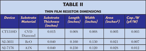
Table 2 compares the physical sizes of each chip thin film resistor. As seen from the Table, the C/W ratio of the CVD diamond chip is significantly lower than that of conventional substrate materials.

Figure 1 VSWR vs. frequency for different terminations.
The reduced capacitance per watt of CVD diamond has many advantages for RF circuits and also translates to higher frequency of operation. Figure 1 shows the measured VSWR of these three chip terminations. For comparison purposes, the frequency at which the VSWR increases above 1.25 is noted. The CVD diamond operates up to 12.4 GHz before crossing the VSWR limit. The AlN chip operates to 3179 MHz before crossing the VSWR limit. The BeO chip operates to 4505 MHz before crossing the VSWR limit.
Common Applications of Diamond RF Resistives
Due to the distinct benefits of CVD diamond, it is worthwhile to present some common applications where this product line has solved design engineering problems, specifically Wilkinson combiners/dividers, isolator circuits and amplifier feedback networks.

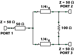
Figure 2 Traditional Wilkinson divider/ combiner.
High Power Wilkinson Power Dividers/Combiners
Figure 2 shows the highly popular single stage Wilkinson divider/combiner.1 High power dividers/combiners require a high power resistor to provide isolation between the combining ports. The isolation resistor can see large amounts of power if the signal at each leg (ports 2 and 3) are out of phase or have unequal amplitudes. The worst case occurs when the signals are 180° out of phase, in which case the isolation resistor will dissipate a majority of the energy. As the trend continues to make RF circuits smaller, the resistor hits a limitation of power dissipation and upper frequency operation. The size reduction of the traditional BeO or AlN resistor is limited due to the substrate thermal conductivity. For a given power rating, the CVD diamond resistor can be made significantly smaller. As shown in Table 2, a 150 W CVD diamond part will have a capacitance per watts ratio of less than half that of the BeO part. This reduced parasitic capacitance allows the combiner with the CVD diamond isolation resistor to operate at a higher frequency with significantly less loss and greater isolation.

Figure 3 S21 vs. frequency for a Wilkinson combiner.

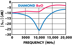
Figure 4 S11 vs. frequency for a Wilkinson combiner.
For comparison purposes, two Wilkinson combiners were designed for a center frequency of 10 GHz (X-band). One combiner uses a 50 W BeO 100 Ω resistor and the other uses a 50 W CVD diamond 100 Ω resistor. Figures 3 and 4 show the S21 and S11 results, respectively. As expected, the BeO resistor has a degraded performance at higher frequencies, due to the shunt capacitance introduced by the resistive film physical size. If using the BeO isolation resistor, a reactive tuning is required to tune out the capacitance for optimized insertion loss and isolation, resulting in a very narrow band combiner and manufacturing repeatability challenges. Diamond resistors have a distinct advantage in this application.

Figure 5 Dual junction circulator duplexer.
Dual Junction Circulator Duplexer Applications
Typical phased array radars, depending on the number of elements, can have hundreds or even thousands of transceivers. Many transceiver topologies require a duplexer for switching between transmit and receive modes. In many cases, the duplexing function is implemented with an isolator in order to isolate the sensitive receive side from any high power transmit crosstalk. In some situations, a dual junction circulator is used to provide isolation up to 50 dB (see Figure 5).2
With this topology, any power that leaks from the transmitter will be absorbed by the 50 Ω termination. The termination resistor must be capable of handling the maximum transmit power, minus the isolation of the isolator. These peak power levels can be extremely high in many radar applications. In the past, these resistors would be large BeO or AlN resistors. The CVD diamond resistor can be used in place of the ceramic resistors. With a smaller size diamond resistor and inherently less capacitance, the duplexer module can be made smaller and the isolator termination port can be better matched to prevent damage to the transmitter. The decreased size of the duplexer is multiplied by the number of array elements, producing a meaningful system size reduction.
Additionally, the decreased capacitance of CVD diamond terminations creates an ideal solution for high frequency radar. As expected, the VSWR of BeO and AlN terminations is degraded at higher frequencies and can ultimately limit the overall performance of the isolator.
In some instances, the 50 Ω termination used for the isolation load can be replaced with a 20 or 30 dB attenuator. This technique is used for power sampling of the power dissipated by the attenuator. This power level can be used as a method of measuring power incident to the attenuator. Similar to the load resistor, the attenuator needs to be sized to handle the worst case reflected power. If implemented with CVD diamond, a size reduction of up to 14 times can be achieved.

Figure 6 Typical FET power amplifier with negative feedback.
Power Amplifier Feedback Resistor
As military and commercial wireless applications begin to stretch across multiple bands, power amplifiers have been required to operate over wider bandwidths. As the bandwidth requirements increase, negative feedback stability compensation becomes necessary.3 Figure 6 shows a simple FET power amplifier with negative feedback. The feedback provides a method of bandwidth improvement and a method of stabilization. In a previous article, the author describes a 0.7 to 1.8 GHz amplifier, which uses a 10 W GaN HEMT and negative feedback.4 The design requires that the feedback resistance be split into two 1206 size resistors, in order to enhance the power handling capabilities. While this may suffice for PA applications to 10 W, higher power amplifiers will require significantly more dissipation capabilities from the feedback resistors. In another article, the author describes a 100 W amplifier using LDMOS transistors with a flanged feedback resistor.5 In this case, the large feedback resistor requires a flanged device to handle the amount of feedback power dissipated in the resistor. This can lead to a physically large design and an increase in shunt capacitance of the resistor, which will load the output of the LDMOS amplifier.
In both amplifier designs, the CVD diamond resistors can offer benefits of greater power handling in a smaller package than the ceramic counterparts resulting in an overall size reduction.
Conclusion
The key system parameters of radar and wireless infrastructure systems are pushing the capabilities of even the simplest of passive components, the resistor. These passive components need to handle more power, at higher frequencies, and with smaller packages. The Diamond RfTM Resistive technology is a proven solution to equip wireless designers with a resistive component that handles more power, at higher frequencies, and is produced in a smaller package.
For more information: http://www.emc-rflabs.com/Passive-Components/Overview.aspx
References
- D.M. Pozar, Microwave Engineering, Third Edition, John Wiley & Sons Inc., Somerset, NJ, 2005, p. 318.
- “Engineering Reference Guide,” Florida RF Labs/EMC Technology, www.emct.com/IMG/pdf/EngGuide2008.pdf, p. 18.
- G. Gonzalez, Microwave Transistor Amplifiers Analysis and Design, Prentice Hall, Upper Saddle River, NJ, 1997, pp. 333-347.
- S. Azam, C. Svensson and Q. Wahab, “Comparison of Two GaN Transistor Technologies in Broadband Power Amplifiers,” Microwave Journal, Vol. 53, No. 4, April 2010, pp. 184-192.
- C.G. Gentzler and S.K. Leong, “Broadband Amplifier Design Utilizing Coaxial Transformers,” Polyfet RF Devices, www.polyfet.com.
- L.G. Maloratsky, “Transceiver Duplexer Design Considerations,” Microwave Journal, Vol. 51, No. 10, October 2008, pp. 68-86.
