In the past ten years, an interest in more accurate characterization of RF MOSFETs has emerged. The rapid advancement of low-cost CMOS silicon process has made possible the application of CMOS technology at radio and microwave frequencies. When conducting S-parameter measurements of microwave devices directly on a wafer, the low silicon substrate resistivity and the characterization of the metal lines are of primary concern.1 Moreover, a characteristic of the low-cost silicon processes is that device performance per unit area is usually low. The test structure must be very large in order to fit the large devices.2 Consequently, the parasitics of the test structure are significant. To reduce the impact of the parasitics of the test structure, several new techniques have recently been adopted, including compensated de-embedding3-5 and a shield-based test structure.2
In this article, a microwave model of the test structure is proposed and its equivalent circuit parameters are determined. In order to reduce the impact of the parasitics on the DUT characteristics, the size of the pads and the width of the interconnection lines of the test structures are analyzed and optimized, based on accurate electromagnetic (EM) simulation. A 0.13 µm RF CMOS process, with eight levels of metallic layer, is used to fabricate the test structures, which are designed according to the optimization result.
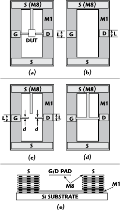
Figure 1 (a) RF test structure containing the DUT; (b) pad test structure; (c) open test structure; (d) short test structure; and (e) cross-section of the test structure.
Test Structure
Because the MOSFET is too small to be contacted directly, measuring its RF behavior with coplanar probes requires a test structure that consists of probe pads and interconnecting lines and the device under test (DUT). The probe pads connect the measurement probe and silicon wafer; the interconnecting lines connect the pads and the DUT. The MOS model parameters are extracted from S-parameter measurements on the test structure.4 The parasitic components, which mainly originate from the probe pads and the metallic interconnecting lines, influence the S-parameter measurements of the DUT. Here, the size of the pads and the width of the lines are analyzed in order to minimize the influence of the parasitics.
A 0.13 µm RF CMOS technology with eight levels of metal interconnects is used to fabricate the test structure. The layout of the MOS test structure and the de-embedding structures are shown in Figure 1. The layout of the pads and the interconnecting lines is identical for the test structure and the de-embedding structures. The length of the test structure is 235 µm and the width is 230 µm. Starting on the left hand side, there are input pads in GSG arrangement with 100 µm pitch and output pads with the same configuration as input pads.
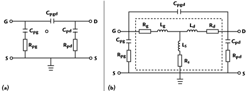
Figure 2 Equivalent circuits: (a) open structure and (b) short structure.
Extraction Methodology for the Parasitic Parameters
The equivalent circuits of the open structure and of the short structure are shown in Figure 2.7 Cpg and Cpd represent the pad capacitance of the gate and drain between the signal pad and the ground pad, respectively. Cpgd represents the coupling capacitance between the gate and drain pad. Rpg and Rpd represent the substrate loss resistance of the gate pad and the drain pad, respectively. Lg, Ls and Ld represent the inductance of the gate, source and drain interconnecting line, respectively. Rg, Rs and Rd represent the resistance of the gate, source and drain interconnecting line, respectively. L is the length of the signal pads and d is the width of the metallic interconnecting lines.8 All the parameters can be determined by using several steps as follows:
(1) Parameter Extraction of the open test structure:

where Yopen is the matix obtained from conversion of the measured S-parameters of the open test structure. Provided that (ωRpgCpg)2+1≈1, then


From Equations 2 and 4, one can get


(2) Parameter Extraction of the short test structure:

where Yshort is the matrix obtained from conversion of the measured S-parameters of the open test structure and Yshort1 is the Y-parameter of the dashed box part of the equivalent circuit.

where Zshort1 is the Z-parameter matrix obtained from the conversion of Yshort1. Then one can get the expressions of Rs, Rg, Rd, Ls, Lg and Ld as follows:


EM Analysis
At RF and microwave frequencies, the geometrical size of the test structure is close to the wavelength of the electromagnetic waves. The influence of electromagnetic interaction and radiation on the characteristics of the DUT increases. Electromagnetic interaction and radiation can be included in the equivalent circuit model of the test structure by an analysis technique based on EM simulation. The conventional approach, which adopts the lumped elements modeling technique, is unable to predict the characteristic of the different size structures. The relationship between the size of the test structure and the extrinsic elements of the equivalent circuit model can be analyzed and predicted by an EM simulation analysis technique before the test structure is fabricated, so that the parasitics can be alleviated as much as possible.6
Here, the commercial software HFSS is used to characterize the test structures and their S-matrix parameters are obtained. The test structure is characterized through its scattering matrix SEM, which is computed by means of EM simulation on the basis of device geometry and material parameters. Thus, EM propagation and coupling effects are considered for the test structure. Once the scattering matrix SEM of the test structure has been obtained, the Y parameters can be deduced from the SEM. The value of all the components of the test structure can then be extracted.
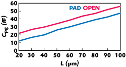
Figure 3 Cpgvs. the length of the pads.
The Pad Capacitance
It is theoretically obvious that the pad capacitance is dependent on the size of the signal pads. Figure 3 shows the relationship between the size of the signal pads and the capacitance Cpg. It is clearly seen that Cpg is directly proportional to L, the length of the signal pads, which are extracted from SEM, the EM simulation result of the test structure. The characteristic of Cpd is identical with that of Cpg. The reason that the capacitance value of the open structure is bigger than that of the pad structure is that there is a coupling capacitance between the metallic interconnecting lines and the Si substrate in the open structure. In order to reduce parasitic capacitance, the size of the signal pads must be decreased, whereas the size of the pads should be bigger than that of the probe pinpoint.

Figure 4 (a) Lg, Rg vs. d and (b) Cpgd vs. d.
The Parasitic Resistance and Inductance of the Interconnecting Lines
Figure 4 shows the relationship between the parasitic inductance and resistance of the interconnecting lines versus d, the width of the lines, which are extracted from the EM simulation result9 and the coupling capacitance between the two signal pads. It is clearly seen that the parasitic resistance and inductance is inversely proportional to the width of the lines, whereas the coupling capacitance between two signal pads is directly proportional to d.
The Coupling Capacitance Between the Input and Output
The coupling capacitance Cpgd relates to the location and width of the interconnecting lines of the input and output signal pads. Figure 5 shows the bilateral and the central symmetry of the gate and drain interconnecting lines. Figure 6 shows the value of Cpgd extracted from EM simulation results. The conclusion can be drawn that the layout with central symmetry is better than the lateral symmetry, because the value of Cpgd is smaller.
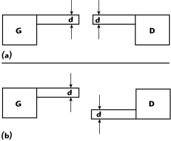
Figure 5 Layout of the input and output interconnecting lines of the pads: (a) bilateral symmetry and (b) central symmetry.
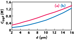
Figure 6 Coupling capacitance between input and output pads: (a) lateral symmetry and (b) central symmetry.
Parameter Extraction and Discussion
After the above analysis, some important conclusions can be drawn regarding the relationship between the size of the test structure and the value of the parasitic elements:
1) The length L of the signal pads should be shortened in order to reduce the value of Cpg and Cpd. Because the size of the pads should be larger than that of the probe point, L was set Cpd equal to 35 µm.
2) In order to reduce the effect of the parasitics of the interconnecting lines between the input and output pads, the width of the gate, drain and source lines were set to 10, 16 and 30 µm, respectively.
3) In order to reduce the coupling capacitance Cpgd, the layout with a central symmetry of the gate and drain interconnecting lines was chosen.
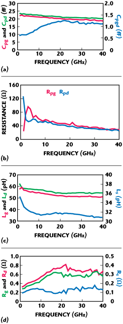
Figure 7 Frequency characteristics of: (a) Cpg, Cpd, Cpgd; (b) Rpg and Rpd; (c) Lg, Ld and Ls; and (d) Rg, Rs and Rd.
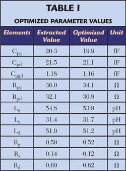
The test structures have been fabricated and measured in accordance with the dimensions determined above. The parameters of the test structures have been extracted based on Equations 5 to 9 and 13 to 17.10 Figure 7 shows the frequency characteristics of all the parameters. All the parameters are optimized with Agilent ADS. Table 1 shows the extracted and optimized values of the parameters of the test structure.

Figure 8 Measured and simulated S-parameters of the short test structure: (a) S22, (b) S12, (c) S21 and (d) S22.
Figure 8 compares the simulated and measured reflection and transmission coefficients, up to 40 GHz for the short test structure. From these figures, it is observed that relatively good agreement between measured and simulated data can be achieved. However, it is noted that the differences between simulated and measured values of S12 and S21 at the higher frequency range are larger than those at the lower frequency range due to the increasing parasitic effects such as EM coupling and unintended radiation.
The possible cause of the differences between the values of the structure parameters extracted from EM simulations and those from measurements are discussed as follows. First, in the EM simulation, it is assumed that a layer of dielectric is between the pads and the ground metallic layer. In reality, the structures are fabricated with multilayer of different dielectrics. Second, the metallic holes between metallic layers are combined into one hole to simplify the analysis and speed up the computation.
Conclusion
A microwave model of an RF MOSFET test structure is proposed and the test structures are analyzed and optimized based on accurate EM simulation. A 0.13 µm RF CMOS technology with eight levels of metallic layer is used to fabricate the test structures. The equivalent circuit parameters of the test structures are then extracted and optimized based on Agilent ADS. Good agreement between the measured and ADS simulated results is obtained up to 40 GHz.
Acknowledgments
This work is supported in part by the Open Research Program of the state Key Laboratory of Millimeter Waves, Southeast University, no. K201002. The authors would like to thank Shanghai SMIC for supplying the test structures and Ms. Xiaofang Yao for measuring the test structures.
References
- J.L. Carbonéro, G. Morin and B. Cabon, "Comparison between Beryllium-copper and Tungsten High Frequency Air Coplanar Probes," IEEE Transactions on Microwave Theory and Techniques, Vol. 43, No. 12, December 1995, pp. 2786-2793.
- T.E. Kolding, "Shield-based Microwave On-wafer Measurements," IEEE Transactions on Microwave Theory and Techniques, Vol. 49, No. 6, June 2001, pp. 1039-1044.
- T.E. Kolding, "A Four-step Method for De-embedding Gigahertz On-wafer CMOS Measurements," IEEE Transactions on Electron Devices, Vol. 47, No. 4, April 2000, pp. 734-740.
- E.P. Vandamme, D.M.M.P. Schreurs and G. van Dinther, "Improved Three-step De-embedding Method to Accurately Account for the Influence of Pad Parasitics in Silicon On-wafer RF Test Structures," IEEE Transactions on Electron Devices, Vol. 48, No. 4, April 2001, pp. 737-742.
- J. Gao, RF and Microwave Modeling and Measurement Techniques for Field Effect Transistors, SciTech Publishing, Raleigh, NC, 2010.
- V. Subramanian, Z. Zhang, D. Gruner, F. Korndoerfer and G. Boeck, "Analysis and Characterization of Microstrip Structures up to 90 GHz in SiGe BiCMOS," 2007 European Microwave Conference Digest, pp. 512-515.
- M. Koolen, J. Geelen and M. Versleijen, "An Improved De-embedding Technique for On-wafer High-frequency Characterization," Proceeding of the BCTM, 1991, pp. 188-191.
- J. Gao and A. Werthof, "Direct Parameter Extraction Method for Deep Submicrometer Metal Oxide Semiconductor Field Effect Transistor Small-signal Equivalent Circuit," IET Microwaves, Antennas & Propagation, Vol. 3, No. 4, 2009, pp. 564-571.
- B.L. Ooi, Z. Zhong and Y. Wang, "A Distributed Millimeter-wave Small-signal HBT Model Based on Electromagnetic Simulation," IEEE Transactions on Vehicular Technology, Vol. 57, No. 5, September 2008, pp. 2667-2674.
- Q. Wang, C. Yuan and Y. Huang, et al., "An Approach for Determining MOSFET Small-signal Circuit Model Parameters," Microwave Journal, Vol. 51, No. 10, October 2008, pp. 116-128.
