Commercially available RF, microwave and optical driver amplifiers provide their best performance under specific bias conditions. The quiescent current of such amplifiers affects critical performance parameters such as efficiency, inter-modulation distortion products and noise figure. Therefore, it is crucial to bias these amplifiers accurately for best performance. Some amplifier manufacturers provide optimum bias conditions via conventional integrated self-biasing schemes such as resistor division. Although simple in implementation, these solutions cannot compensate for the amplifiers' process, part to part and temperature variations, sacrificing performance and efficiency.
In order not to degrade performance, RF engineers usually employ an active bias control scheme. The active bias control circuit measures the current passing through the amplifier to allow compensation for any possible drift. Such control circuits are complicated and require not only multiple external components (LDOs, charge pumps, voltage sequencing and protection circuits), but also expensive calibration cycles in production. Such implementations occupy a large PCB area, usually much larger than the amplifier itself. Since each amplifier requires a different drain (collector) and gate (base) bias setting, the external bias circuitry is often redesigned for each amplifier, significantly increasing time to market. The HMC920LP5E houses all the necessary operation blocks in a compact 5 × 5 mm QFN SMT package. This results in PCB area reduction of up to 70 percent, compared to the discrete biasing implementations, by eliminating multiple IC and external component requirements.
In order to increase efficiency, many systems use amplifiers operating in saturation where they require large gate currents in deep saturation (P3dB). Moreover, many amplifiers' gate current changes direction when it is pushed into deep saturation. When the amplifier is in the linear region, the current is negative (i.e., out of the gate). However, when the amplifier goes into saturation, the Schottky diodes turn on, reversing the direction (into the gate) for the exponentially growing current. Hence, the bias circuitry should be able to handle both current sink and source to the gate.

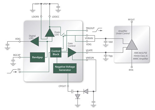
Figure 1 HMC920LP5E applications block diagram.
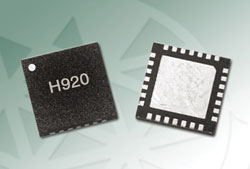
With all these design challenges, designing the bias section for the amplifier chain is generally the most time consuming step in development. Hittite has recognized this problem and successfully developed the industry's first monolithic biasing solution: the HMC920LP5E Active Bias Controller. This new IC provides a compelling combination of an active bias controller that generates a regulated drain and gate voltage, along with an on-chip negative voltage generator that can be utilized when a negative voltage is needed (e.g., depletion mode devices). This unique and timely solution by Hittite is offered in a compact 5 × 5 mm QFN leadless package. A behavioral block diagram of the HMC920LP5E with the external and connections for standard set of features are given in Figure 1.

The HMC920LP5E requires only a dual schottky, and a few external passive components in standard configuration. The main feature, active bias control loop, continuously monitors the current through the external amplifier to generate the gate voltage VGATE. The provided feedback control scheme is thus enforcing constant quiescent bias for the amplifier under control. Table 1 provides a complete list of standard and optional features of the HMC920LP5E and its benefits.

Figure 2 HMC920LP5E's excellent PSRR provides spur-free RF spectrum (A) compared to discrete biasing spectrum (B).
The HMC920LP5E achieves excellent bias stability over system supply (+4 to +16.5 V), temperature (-40° to +85°C) and process variations, eliminating the otherwise required calibration procedures. The HMC920LP5E is a versatile turn-key bias solution, for biasing any enhancement and depletion type amplifier operating in a Class A regime with drain voltages (VDRAIN) from +3 to +15 V and drain currents (IDRAIN) up to 500 mA. The user-adjustable VDRAIN output is used as the regulated supply rail for the amplifier. The VGATE driver is designed to handle both source and sink currents up to ±4 mA to ensure proper bias control even in deep saturation.
The HMC920LP5E includes a regulated charge-pump to produce a negative supply rail of -2.5 V (VNEGIN) for the gate driver. The smart control of the integrated charge pump provides low ripple regulated output with limited spike currents. The on-chip gate driver has an excellent PSRR and rejects the inherent ripple on the VNEGIN even further. This unique feature of the HMC920LP5E provides a spur-free RF spectrum, giving better noise performance compared to discrete biasing solutions. Figure 2 shows the comparison of the RF spectrum for the same amplifier biased with HMC920LP5E versus a discrete biasing circuitry.

Figure 3 HMC920LP5E active bias controller driving a HMC465LP5E amplifier.
The HMC-920LP5E ensures the safety of the amplifier under control by a special power-up sequence either from a fresh start-up, as seen in Figure 3, or enabling the active bias control by toggling enable pin (EN), as seen in Figure 4. At start-up, V-DRAIN is pulled down to GND until the VNEGIN settles down to -2.5 V. VGATE is then pulled down to the most negative supply available to ensure that the amplifier under control is completely turned off. Once VGATE reaches VNEGIN, VDRAIN is turned on and active bias loop is enabled. The final phase of the power-up sequence is increasing the VGATE linearly until the target value for IDRAIN is reached.

Figure 4 Enable/ disable waveform.
The amplifier under control can be enabled or disabled using the EN pin of the HMC920LP5E, as shown in Figure 4. When disabled through this pin, only the VGATE and VDRAIN outputs will be affected; the rest of the chip (negative voltage generator, bandgap, high voltage LDO output LDOCC) will remain operational.
The HMC920LP5E has multiple operation modes and can be configured to control both enhancement and depletion mode devices. In the depletion mode configuration the HMC920LP5E is capable of internally generating a negative voltage as well as operating from an external negative supply voltage. The HMC920LP5E also allows designers to implement custom daisy-chain power-up sequencing in cascaded amplifier systems, as shown in Figure 5. In this example, three cascaded amplifier stages are triggering one another from right to left when quiescent bias is achieved. The HMC920LP5E will thus ensure a safe and controlled turn on/off of the cascaded amplification stages.

Figure 5 Daisy chain operation.
The HMC920LP5E incorporates multiple warning and protection features that could not be easily implemented using discrete components. The HMC920LP5E continuously monitors the quiescent current of the amplifier and the digital alarm signal, CURALM, output flags when an under/over condition is detected. Similarly, the VDDALM digital output is an indicator for under-voltage condition on the main system supply. The HMC920LP5E also utilizes automatic protection features like power fold back and short circuit protection to ensure both its own and the amplifier's safety. Under fault conditions such as shorts on VDRAIN, VGATE or VNEGIN, the system goes to the stand-by mode until the fault condition is removed.

Ideal for biasing Class A amplifiers in cellular/3G, WiMAX/4G, VSAT, MW radio, military, fiber optics and test equipment applications, the HMC920LP5E active bias controller is housed in a compact, RoHS compliant 5 × 5 mm QFN SMT package, and is specified for operation from -40° to +85°C (see Table 2). Built on a robust, production qualified, high volume CMOS process, and with its patent-protected unique features, the HMC920LP5E is an excellent solution for various biasing needs. Samples and evaluation PC boards are available from stock. Data sheets and supporting information for the HMC920LP5E and all Hittite products are available online.
Hittite Microwave Corp.,
Chelmsford, MA
(978) 250-3343,
www.hittite.com
RS No. 301
