Semiconductors / Integrated Circuits

IGaN-10-26-20.jpg

IGaN Achieves Low-Conduction Loss with 150 mm GaN-on-Si Epiwafer for RF Applications

Findings pave the way for commercialisation of RF Epistack on 200 m substrates to be commercially available end Q1 2021

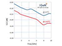
IGaN’s technology has the unique advantage of achieving very low conduction loss meeting the industry standards for GaN HEMT on Si for RF applications. Recently processed IGaN's 150 mm GaN on Si HEMT wafers have achieved a conduction loss of 0.15 dB at room temperature and 0.23 dB at high temperature for an operating frequency of 10 GHz.


Read More
NXP GaN Fab

NXP Advances 5G with New Gallium Nitride Fab in Arizona

High-volume manufacturing facility is the most advanced GaN fab for RF in the United States

NXP Semiconductors N.V. (NASDAQ: NXPI) today announced the grand opening of its 150 mm (6-inch) RF Gallium Nitride (GaN) fab in Chandler, Arizona, the most advanced fab dedicated to 5G RF power amplifiers in the United States. The new internal factory combines NXP’s expertise as the industry leader in RF power and its high-volume manufacturing know-how, resulting in streamlined innovation that supports the expansion of 5G base stations and advanced communication infrastructure in the industrial, aerospace and defense markets.


Read More