
Advantages and Applications of GaN Push-Pull Amplifiers
Gallium Nitride (GaN) has emerged as the preferred high-power amplifier (HPA) technology due to its superior properties compared to LDMOS technology. GaN enables wider bandwidth and higher efficiency amplifier designs, allowing a single wideband amplifier to replace multiple narrowband amplifiers. This reduces board space without sacrificing performance. While a wideband amplifier design offers advantages in terms of space and cost, its broad bandwidth presents challenges in meeting harmonics requirements.
Push-pull power amplifier (PA) topology is gaining popularity as the architecture of choice for many applications like land mobile radios (LMR) and tactical radios. This topology combines two or more PAs to achieve higher power output, resulting in improved efficiency, lower distortion and reduced power dissipation. This also simplifies thermal management challenges.
This article discusses various wideband GaN amplifier topologies and demonstrates why push-pull topology is the ideal solution for optimal performance in wideband PA designs. It compares the pros and cons of a HPA design using two push-pull PAs combined with a 90-degree hybrid versus two PAs combined with baluns. Additionally, the article addresses the specific requirements of low-power and high-power LMR handsets in terms of efficiency, distortion, power handling and thermal management. The article explains how push-pull amplifiers can reduce overall system size while maintaining these critical parameters. It will also present measured performances of recent designs of low-power and high-power push-pull amplifiers that use existing PAs from TagoreTech to address the challenges faced in LMR handset applications.
HPA TECHNOLOGIES
GaN and LDMOS are two of the most common semiconductor process technologies for PA design. With an ever-increasing demand to reduce the size, weight, power and cost (SWaP-C), GaN is rapidly replacing LDMOS in many new PA designs. This is, in part, because LDMOS transistors are typically built on a silicon substrate, while some advanced designs may use silicon-on-insulator substrates.
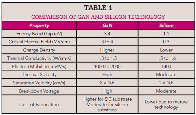
Due to its material properties, GaN offers several advantages over silicon. Table 1 highlights the basic material properties of both GaN and silicon. The properties listed in Table 1 show that GaN devices have much higher power density due to a higher breakdown voltage, saturation velocity and charge density. This higher power density enables GaN devices to be significantly smaller for the same output power, reducing all device capacitances compared to existing LDMOS technology. Lower input and output capacitances facilitate the realization of broadband matching networks. Additionally, higher voltage operation increases the load line impedance for a desired output power, further aiding in the realization of broadband output matching. These factors make GaN an excellent choice for PAs, RF components and functions in other demanding electronic systems where performance and reliability are critical.
BROADBAND PA TOPOLOGIES AND TRADE-OFFS
Broadband PAs are essential components across a wide range of applications, enabling effective communication, enhancing signal quality and ensuring reliability in various fields, from telecommunications to consumer electronics and beyond. The performance of these PAs enables them to handle a broad frequency range, making them versatile components in modern communication systems. Several broadband PA topologies are available, each with its advantages and disadvantages. Some important topologies include:
Lossy Matched Amplifier or Multistage Lumped Element Matching: This topology employs multistage input and output matching networks with lumped elements like resistors, capacitors and inductors to achieve wider bandwidth.
Feedback Amplifier: Negative feedback is applied to extend the bandwidth. Both shunt and series feedback configurations have been used in this context, but shunt feedback generally yields the best results.
Distributed Amplifiers: This topology uses the concept of “additive amplification” with multiple transistors and offers ultra-broadband operation that can extend from DC up to the cutoff frequency of the active devices.
Push-Pull Amplifiers: A push-pull amplifier configuration uses two active devices to address the positive and negative cycles of an input signal. This design improves efficiency and reduces distortion by canceling even-order harmonics, making it particularly effective in audio and RF applications. By alternating the conduction between the two devices, push-pull amplifiers can deliver high output power while maintaining good linearity and thermal performance. Complementary operation, reduced distortion and improved thermal stability contribute to the overall bandwidth improvement of push-pull amplifiers.
Table 2 summarizes the comparison of different broadband PA topologies. Distributed amplifiers typically offer the maximum bandwidth among the four types of PA topologies listed. This makes them suitable for applications requiring very wide frequency coverage. Push-pull amplifiers and feedback amplifiers can also provide extended bandwidth but generally do not reach the same levels of bandwidth as distributed amplifiers.
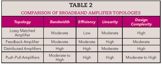
When considering distortion, efficiency and other factors like bandwidth, both push-pull and distributed amplifiers have their strengths. However, push-pull amplifiers stand out in terms of efficiency, ease of design, reduced distortion, better heat management and lower costs. This makes them an excellent option for high-power applications, such as tactical radio and LMR systems.
GaN push-pull PAs have distinct advantages over other technologies due to the properties of GaN. This amplifier topology/technology choice delivers better efficiency, wider bandwidth, higher power density and improved thermal performance. Overall, these benefits make GaN push-pull amplifiers an appealing option for various applications, including telecommunications, aerospace and defense systems.
PUSH-PULL DESIGN APPROACH
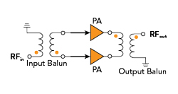
Figure 1 Push-pull PA block diagram.
The push-pull design approach uses two transistor or HEMT-based devices to amplify an input signal. In this setup, one device handles the positive half of the waveform while the other manages the negative half. Figure 1 shows the basic building block of a push-pull PA.
The key components of a push-pull PA are:
Input Stage: The input signal is typically differential, coming from a source that can produce balanced outputs. A balun converts the single-ended unbalanced signal into two equal but opposite phase-balanced signals that drive the two active devices.
Active Devices: Two active FETs or HEMTs are arranged in a push-pull configuration. Each device handles one half of the input waveform. One amplifies the positive half, while the other amplifies the negative half.
Balun: A balun is located at the input and output of the PA. At the input, the balun translates the single-ended signal into a differential signal. At the output, it translates the differential signal back into a single-ended signal. The balun can also be designed to provide impedance transformation for the desired bandwidth. It helps in minimizing common-mode noise and ensures that the power is evenly distributed between the two devices.
Output Stage: The outputs of the two transistors are combined at the output stage. The balun ensures that the combined output is in phase and delivers the amplified signal to the load.
Feedback Mechanism (optional): Feedback can be implemented to improve linearity and reduce distortion. It may be applied from the output back to the input stage, stabilizing the overall gain.
The input signal enters the amplifier, where the balun converts it into two balanced signals. The two active devices amplify their respective halves of the signal. The amplified outputs are fed into the balun, which combines them into a single unbalanced output. The output is delivered to the load (e.g., an antenna), providing high power with low distortion. The architecture of a push-pull PA using a balun effectively combines the benefits of balanced operation and push-pull design, resulting in high efficiency, low distortion and broader bandwidth.
CRITICAL BALUN PARAMETERS
The design/selection of the balun is one of the most critical factors in the design of push-pull PAs. Several factors need to be considered when designing or selecting the correct balun for the amplifier design:
Operational Bandwidth: The bandwidth where the balun must meet the specified requirements.
Insertion Loss: A critical parameter that directly impacts the overall efficiency of the amplifier. Higher insertion loss also limits the power handling capability of the balun and may make thermal management challenging.
Amplitude and Phase Imbalance: Directly impacts the achievable common-mode rejection ratio (CMRR) of the balun.
Impedance Transformation Ratio: The desired ratio between the input and output impedances.
Power Handling: The maximum power the balun can handle without exceeding its specified limits.
A CMRR of 20 to 25 dB is commonly achievable in a balun over a wide bandwidth. Figure 2 shows a chart of CMRR versus phase and amplitude imbalance. This chart shows that a balun must have less than 0.5 dB of amplitude imbalance and 5 degrees of phase imbalance to achieve 25 dB CMRR. These imbalance values need to be measured at the even-order harmonic frequencies.
The maximum power requirements of the amplifier drive the maximum power handling requirements of the baluns. Higher power baluns that are used on the PA output will typically be larger due to thermal management considerations. This is a critical factor when designing baluns.
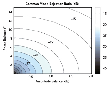
Figure 2 CMRR versus amplitude and phase imbalance. (credit: “Balun Basics Primer,” Marki Microwave, May 5, 2023).
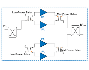
Figure 3 Push-pull PA using hybrid 90° couplers.
HIGH-POWER BROADBAND PA DESIGN
For broadband high-power applications, a single high-power device may be used to design a single-ended PA to meet specifications. However, using a single high-power device presents challenges with bandwidth, PAE, harmonics, thermal management and cost. To minimize harmonics, lowpass filters (LPFs) are needed to suppress the harmonics generated by the PA. LPF components must support the appropriate power levels, which may increase their size and the space required on the PCB. This adds to the loss and cost of the overall design. Additionally, achieving better PAE and output power with a single PA often requires sacrificing output return loss. Standard designs using a single high-power PA also typically achieve poor second harmonic levels.
Alternatively, using two smaller PAs in a push-pull topology and combining them with a 90-degree hybrid, as shown in Figure 3, can yield higher Pout, improved PAE, better harmonic performance and excellent input and output return loss due to the inherent characteristics of the hybrid. This approach enhances overall performance and addresses the efficiency issues associated with single high-power device designs. This topology also simplifies thermal management efforts since power dissipation is distributed across four active devices rather than one in the single-device HPA. One of the drawbacks of this push-pull topology is cost, as it requires additional baluns and hybrid combiners at the input and output.
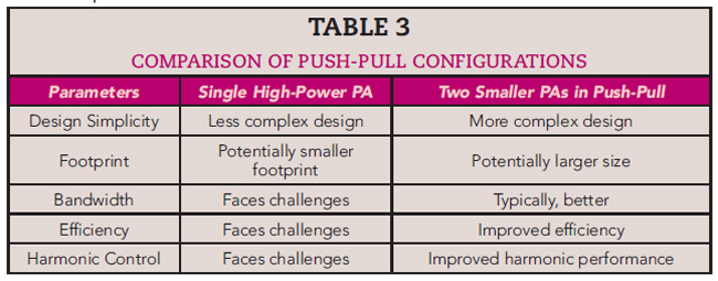
Table 3 summarizes the comparison of a single PA configuration versus two small push-pull PAs. Table 4 summarizes the comparison of a single HPA versus two push-pull PAs combined with a 90-degree hybrid.
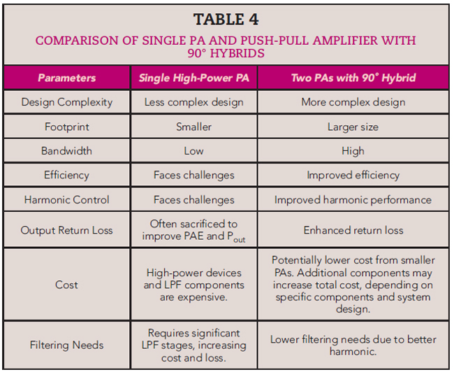
Overall, the push-pull topology with 90-degree hybrids offers a more efficient and higher performing solution for high-power broadband PA design despite the increased design complexity and potential for higher costs.
PUSH-PULL AMPLIFIER REFERENCE DESIGNS
To illustrate the practical application of the push-pull PA design approach, this section presents 15 W and 65 W push-pull PA module reference designs.
15 W Push-Pull PA Module
Figure 4 shows a 15 W push-pull amplifier design using TagoreTech’s TA9310E GaN-on-SiC power transistors and baluns. This amplifier is designed to operate from 30 to 512 MHz. The two GaN HEMTs are biased at an 18 V drain supply with a total quiescent current of 80 mA. The input side of the module uses a balun rated at 1 W, while the output uses a balun from Mini-Circuits rated at 15 W.
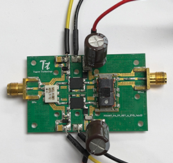
Figure 4 15 W push-pull PA module.
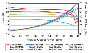
Figure 5 15 W PA module gain and PAE.
The push-pull design effectively minimizes second-order harmonics to -35 dBc without sacrificing output power or PAE. The desired levels of power and PAE can be achieved by operating the push-pull amplifier at drain voltages below the maximum rating for the GaN PA. The reduction of second-order harmonics makes this design particularly advantageous for tactical radio applications, especially within the 30 to 512 MHz frequency band. The GaN power transistors shown in Figure 4 are mounted on an evaluation board developed by TagoreTech. This module delivers an average power output of approximately 15 W. Figure 5 shows the measured gain and PAE versus output power for the 15 W PA module. Figure 6 shows the performance of the second-order harmonics versus the output power of the 15 W amplifier module.
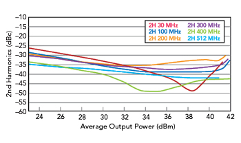
Figure 6 15 W PA module second-order harmonics.

Figure 7 65 W push-pull PA module.
65 W Push-Pull PA Module
Figure 7 showcases a 65 W push-pull amplifier design developed using two of TagoreTech’s TA9410E 40 W GaN-on-SiC power transistors in conjunction with an in-house coaxial balun design. This amplifier is designed to operate from 135 to 870 MHz, driven by a 50 V drain supply. For optimal performance, a balun rated at 4 to 5 W is utilized on the input side, while a balun rated at 75 W is employed at the output.
The amplifier’s push-pull topology effectively reduces second-order harmonics to -30 dBc. This ensures that output power and PAE are not compromised. Operating at a maximum voltage of 50 V, this design meets the high-power requirements essential for dash-mount or vehicular LMR/PMR radio applications.
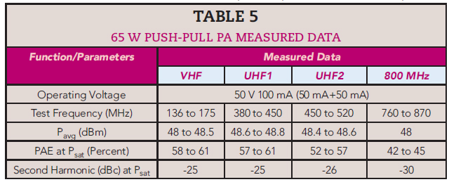
The suppression of second-order harmonics makes this amplifier particularly suitable for LMR applications, especially across very high frequencies (VHF), ultra-high frequency 1 (UHF1), UHF2 and the 800 MHz band. Table 5 shows a summary of the 65 W push-pull amplifier performance in these bands. The evaluation board in Figure 7 delivers an average power output of 63 to 70 W in the LMR frequency range. Figure 8 shows the measured gain and PAE versus output power for the 65 W PA module. Figure 9 shows the performance of the second-order harmonics versus the output power of the 65 W amplifier module.
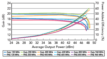
Figure 8 65 W PA module gain and PAE.
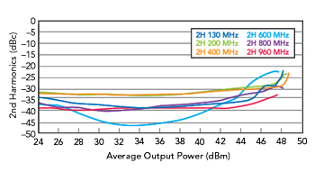
Figure 9 65 W PA module second-order harmonics.
SUMMARY
This article has explored the advantages of push-pull amplifier topology, particularly when combined with GaN technology, for wideband PA design. By pairing two or more amplifiers, push-pull amplifiers effectively address the challenges of achieving high power output, wide bandwidth and low distortion in broadband PA designs. GaN technology offers superior properties such as wide bandwidth, high efficiency, superior thermal conductivity and high breakdown voltage, making it an ideal choice for these applications.
The article has compared push-pull configurations to PA designs using a single device. This analysis has highlighted the superior harmonic performance, efficiency and thermal distribution of the push-pull architecture. Despite the increased design complexity and potentially higher component count, push-pull configurations provide significant advantages in bandwidth, efficiency and harmonic control.
Combining push-pull topology with GaN technology results in high performance, wideband amplifiers that meet stringent requirements for efficiency, distortion, power handling and thermal management. This makes them a compelling choice for RF applications where performance, size and cost are critical.
