

Capitalize on Full-Wave Electromagnetic Simulations with 3D EM Component Models
To meet the needs of applications that require small form factors, it may be necessary to build circuits with surface-mount components that are densely packed onto a printed circuit board. In these scenarios, an additional challenge is that components located close to one another may also interact with each other. Unfortunately, these coupling interactions cannot be captured by simulations that include equivalent-circuit models for the components. However, it is possible to capture these coupling interactions by using 3D models in a full-wave 3D electromagnetic (EM) simulation.
This article explains the benefit of using 3D EM simulations combined with 3D models for designs where components are located close to each other. Performing such a simulation allows for a more accurate prediction of the actual performance of these designs. To illustrate this point, two case studies are presented: a design in which components are separated by a considerable distance and another design in which components are located close together. The analysis is carried out by performing planar EM/circuit co-simulations using Ansys® Electronics Desktop and 3D EM simulations using Ansys® HFSS™. All component models used in the examples are included in the Modelithics® COMPLETE+3D Library.
MODELITHICS MICROWAVE GLOBAL MODELS, 3D GEOMETRY MODELS AND 3D BRICK MODELS
The Modelithics COMPLETE+3D Library is a collection of models for components from many popular vendors. Included in this library are Microwave Global Models™, which are measurement-based equivalent-circuit models for capacitors, inductors and resistors.1 These models capture parasitic effects and scale for part values, substrates and solder-pad dimensions.
The Modelithics COMPLETE+3D Library also includes a collection of 3D Geometry Models for components like inductors, capacitors, filters and packages.2 These models are based on physical dimensions and material properties and are intended for use in full-wave EM simulations. The benefit of these 3D models is that they enable designers to predict the effects of coupling that may arise when components are located close to other components or objects.

Figure 1 Simplified bandpass filter schematic.
Finally, the Modelithics COMPLETE+3D Library also includes what are known as 3D Brick Models™ for multi-layer ceramic capacitors (MLCCs).3 A 3D Brick Model is a simplified approximation of a capacitor’s physical geometry. However, these models alone do not account for internal device parasitics. Therefore, when using 3D Brick Models, the complete simulation process involves first performing a 3D EM simulation that includes all 3D Brick Models along with all 3D Geometry Models, if the design also includes 3D Geometry Models. This 3D EM simulation captures any coupling interactions that may exist between components. The next step is to perform a 3D co-simulation in a circuit schematic. This 3D co-simulation incorporates the 3D EM simulation data and combines it with the Microwave Global Model(s) for the corresponding capacitor(s) to allow for a complete 3D EM simulation.
Case Study 1: Filter Without Component Spacing Constraints
For the following analysis, lumped-element bandpass filter designs will be examined. The topology used for the filter designs shown here is known as the equal shunt legs topology. This topology is available as a selection in Ansys NuHertz® FilterSolutions (ANFS), which is a tool that enables users to synthesize various types of filters.4 In the case of lumped-element filters, FilterSolutions lets users choose from different topologies, including classical, equal inductors, equal shunt legs, high/lowpass and others.

Figure 2 Bandpass filter layout where components have ample spacing.
Figure 1 shows a simplified schematic of the filters that will be presented in this case study. The first example considers the case where there is a considerable amount of space between components. Figure 2 shows the layout of the filter with a total length of about 0.929 in. Note that the substrate used is 0.004 in. thick Rogers RO4350B material. The TDK MLG0603P series and the Passive Plus 0201N series, both of which come in a 0201 size, are used for all inductors and capacitors, respectively. Modelithics offers Microwave Global Models for both part series. Finally, Table 1 lists the values of all the inductors and capacitors. For this example, the targeted center frequency is about 1.5 GHz.

The analysis begins by performing a planar EM/circuit co-simulation using Ansys’ 2.5D Method of Moments (MoM) EM solver to simulate the layout shown in Figure 2. A schematic must then be created that includes the planar EM data properly connected to the Microwave Global Models for the MLG0603P inductors and 0201N capacitors. This schematic is shown in Figure 3. Simulating this schematic produces the final planar EM/circuit co-simulation results.

Figure 3 Filter layout planar EM data connected to the Microwave Global Models.
Having discussed the planar EM/circuit co-simulation method, the focus turns to the 3D EM simulation. The planar EM/circuit co-simulation schematic shown in Figure 3 includes Microwave Global Models for the TDK MLG0603P inductors and Passive Plus 0201N capacitors. For the TDK MLG0603P inductor series, Modelithics also offers 3D Geometry Models for inductors ranging from 0.6 to 120 nH. Modelithics also offers a 3D Brick Model for the Passive Plus 0201N capacitor series. Figure 4 shows the bandpass filter of Figure 2, populated with the components of Table 1 in Ansys HFSS with 3D Geometry Models for the TDK inductors and 3D Brick Models for the Passive Plus capacitors.

Figure 4 HFSS bandpass filter design with 3D Geometry Models and 3D Brick Models.

Figure 5 Schematic used for the 3D co-simulation of the bandpass filter.

Figure 6 One of the (compact) bandpass filters that was built and measured.
Now, a complete 3D EM simulation is possible by first completing a 3D EM simulation in HFSS of the design shown in Figure 4. The next step is to perform a 3D co-simulation that includes the data from the 3D EM simulation properly connected to the Microwave Global Models for the capacitors. The schematic for this model is shown in Figure 5. It includes the 3D EM simulation data, as the center element, connected to the Microwave Global Models for the capacitors. Simulating this schematic produces the final 3D EM simulation results.
To confirm the measured versus modeled results, the bandpass filter was built and measured. Figure 6 shows the assembled filter including the same inductors and capacitors from the simulations. Figure 7 shows the results obtained from the planar EM/circuit co-simulation and the 3D EM simulation along with the measured data of the filter. The solid red trace represents the planar EM/circuit co-simulation results, while the solid blue trace corresponds to the 3D EM simulation results. The dashed traces represent the measured data of three filters.

Figure 7 Simulated and measured S21 of the bandpass filter.
Figure 7 reveals that the planar EM/circuit co-simulation and 3D EM simulation produce similar results. A slight difference does exist, as the planar EM/circuit co-simulation produces a frequency response that is shifted roughly 40 MHz lower than that produced by the 3D EM simulation. Figure 7 also shows how the measured data follows the 3D EM simulation results more closely than the planar EM/circuit co-simulation results. Since both simulations produce similar results, coupling interactions do not appear to be significant. While the 3D EM simulation provides a good prediction of actual performance, the planar EM/circuit co-simulation still adequately predicts actual performance.

Figure 8 Bandpass filter layout with densely packed components.
Case Study 2: Filter With Densely Packed Components
The next case study analyzes a similar bandpass filter. The major difference between this filter and the one analyzed previously is that the components are located very close to each other in this design. Figure 8 shows the layout of this filter. In this case, the total length is only about 0.361 in. Note that the same 0.004 in. thick Rogers RO4350B substrate is used for this design. While this design offers the benefit of smaller size, it also comes with the challenge of greater coupling interactions between components.

The target center frequency for this design is 1.46 GHz. Table 2 lists the part values of the inductors and capacitors. Again, the TDK MLG0603P series and the Passive Plus 0201N series are used for all inductors and capacitors, respectively.

Figure 9 HFSS compact bandpass filter design with 3D Geometry Models and 3D Brick Models.
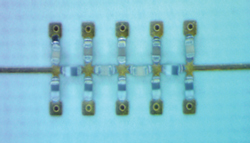
Figure 10 One of the (compact) bandpass filters that was built and measured.
The analysis for this case study is the same as the previous design example. Both a planar EM/circuit co-simulation and a 3D EM simulation are performed as described earlier. Figure 9 shows the bandpass filter in HFSS with 3D Geometry Models for the inductors and 3D Brick Models for the capacitors.
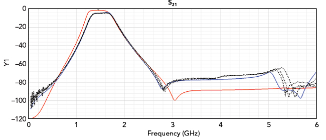
Figure 11 Simulated and measured S21 of the compact bandpass filter.
Figure 10 shows the assembled filter including the inductors and capacitors from the simulations. Figure 11 shows the simulated and measured S21 of this compact bandpass filter. Again, the solid red trace represents the planar EM/circuit co-simulation results, the solid blue trace corresponds to the 3D EM simulation results and the dashed traces represent the measured data of three filters. Figure 12 shows the simulated and measured S11 of the compact bandpass filter over a DC to 6 GHz frequency range and Figure 13 shows the simulated and measured S21 of the bandpass filter over the narrower, 0.5 to 3.5 GHz frequency band. In both figures, the solid red trace represents the planar EM/circuit co-simulation results, the solid blue trace corresponds to the 3D EM simulation results and the dashed traces represent measured data of three filters.
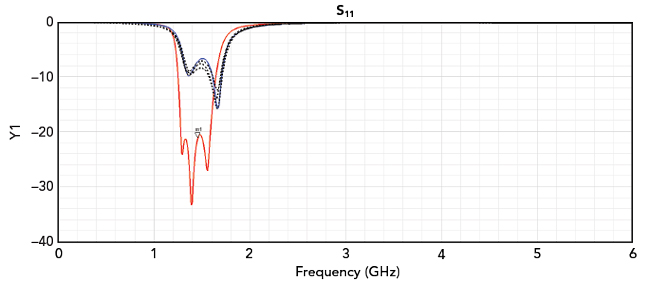
Figure 12 Simulated and measured S11 of the compact bandpass filter.
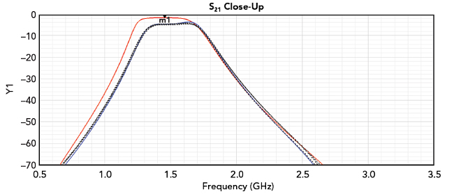
Figure 13 Narrower band simulated and measured S21 of the compact bandpass filter.
Initially, the targeted center frequency of this filter was set at 1.46 GHz. This goal is met considering only the planar EM/circuit co-simulation results. If this were the only verification result, the designer would conclude that the filter design met the requirements and no further action is needed. However, as already shown, the measured data is noticeably different than what the planar EM/circuit co-simulation is predicting. Specifically, in comparison to the planar EM/circuit co-simulation results, the measured data exhibits a reduced bandwidth and higher loss throughout much of the passband. At the desired center frequency of 1.46 GHz, indicated by the m1 marker in the plot, the measured data exhibits poor S11 performance.
This analysis demonstrates how a designer may be unpleasantly surprised when only relying on a planar EM/circuit co-simulation to predict the actual performance of a densely packed design such as this one. On a positive note, the 3D EM simulation results do agree very well with the measured data. These results demonstrate the need for and advantage of using 3D models in a 3D EM simulation for designs in which components are densely packed.
In practice, since the design goal is not being met, the filter would be tuned to achieve the desired performance. This task can be accomplished within the 3D co-simulation schematic from Figure 5. Recall how the 3D co-simulation schematic includes the 3D EM simulation data connected to the Microwave Global Models for the capacitors. Therefore, it is possible to tune the filter by simply adjusting the values of the capacitor models within the circuit schematic. Since the 3D EM simulation data is already incorporated into the schematic, there is no need to perform multiple time-consuming EM simulations.

In this case, the filter can be tuned to achieve the desired performance by adjusting all the capacitor values. Table 3 lists the components used in this tuned version of the compact filter design. Figure 14 shows the simulated and measured S21 of the tuned compact bandpass filter. Figure 15 shows the simulated and measured S11 of the tuned compact bandpass filter over the DC to 6 GHz range and Figure 16 shows the simulated and measured S21 of the tuned bandpass filter over the narrower 0.5 to 3.5 GHz frequency band. Once again, the legend for the curves is the same. The solid red trace represents the planar EM/circuit co-simulation results, the solid blue trace corresponds to the 3D EM simulation results and the dashed traces represent measured data of three filters.
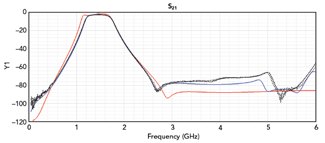
Figure 14 Simulated and measured S21 of the tuned compact bandpass filter.
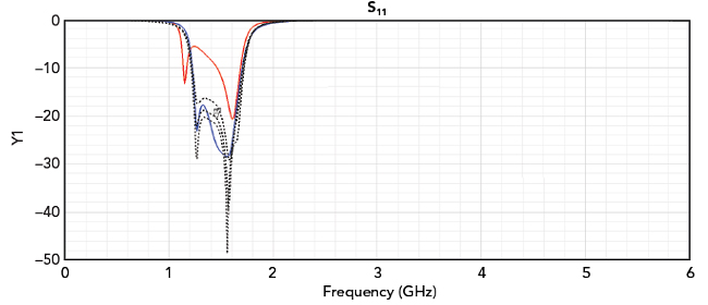
Figure 15 Simulated and measured S11 of the tuned compact bandpass filter.
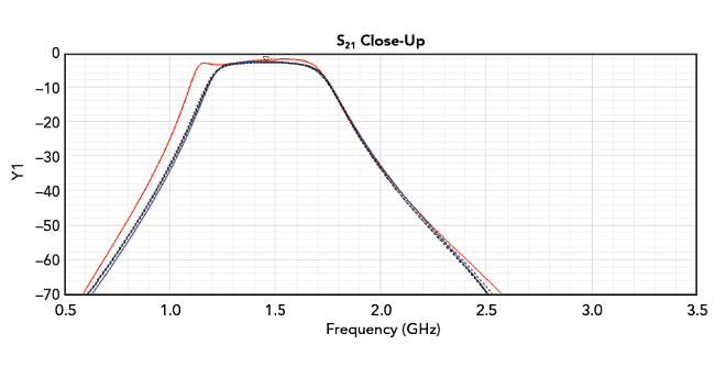
Figure 16 Narrower band simulated and measured S21 of the tuned compact bandpass filter.
The performance curves in Figures 14, 15 and 16 illustrate how the 3D EM simulation accurately predicts the actual performance. This time, the design goal is being achieved with the measured data showing a center frequency of 1.46 GHz. At 1.46 GHz, the measured S11 is lower than -20 dB. The planar EM/circuit co-simulation results again deviate from the measured data. Specifically, compared to the measured data, the planar EM/circuit co-simulation produces a wider frequency response with poor S11 at the low end of the passband.
CONCLUSION
The analysis presented here further emphasizes how 3D EM simulations with 3D models are effective for compact designs. Keep in mind that 3D models are not intended to completely replace equivalent-circuit models. Modelithics equivalent-circuit models like Microwave Global Models are very effective in terms of predicting actual performance when coupling interactions are not playing a major role. For densely packed designs where the effects of coupling may be present, 3D models would be the preferred choice.
References
- C. DeMartino, “Application Note 79: Filter Design Flow in Ansys Electronics Desktop with Modelithics Substrate Scalable Models,” Modelithics, Web: www.modelithics.com/Literature/AppNote.
- I. Bedford, E. Valentino and L. Dunleavy, “Application Note 63: Introduction to Modelithics 3D Models in HFSS,” Modelithics, Web: www.modelithics.com/Literature/AppNote.
- I. Bedford, “Application Note 78: Using 3D Brick Models™ for Full-wave EM/Circuit Model Co-simulation of MLCC Capacitors in Ansys HFSS,” Modelithics Web: www.modelithics.com/Literature/AppNote.
- C. DeMartino, “Streamline Filter Design with Ansys NuHertz FilterSolutions and Modelithics Models.” Modelithics, Blog Post, September 2022.