

A Modern HF/VHF/UHF Transceiver for All Applications – What Would it Look Like Today?
Modern RF transceivers represent more than just separated receiver and transmitter functionalities within the same box. In an operational scenario involving several transceivers, even a “perfect” receiver can demonstrate high-end performance only if the spectral purity of the transmit signals is sufficiently high. Therefore, a transceiver design must align major RF parameters and building blocks between transmit and receive paths to form a combined optimized transceiver architecture! In the following, a state-of-the-art “perfect” transceiver architecture is described.
When a receiver and transmitter are operated at different locations and far away from each other, the only relevant receive parameter is sensitivity, while the only relevant transmit parameter is output power. The closer a transmitter is to the receiver, the more significant are additional performance characteristics for both. While the receiver must increase its robustness to withstand the strong transmit signal at its front-end, the transmitter must increase its spectral purity to ensure that no spectral component from the transmit signal falls into an adjacent receive channel.
Overall system performance is determined by the minimum usable frequency offset between a transmit channel and a receive channel with a given decoupling between a receiver and a transmitter operating a given output power.
This so-called co-site situation directly influences the specifications, for example, adjacent channel power ratio for the radio communication equipment. Within a particular frequency band and its typical applications, the operating parameters may lead to a different transceiver architecture when compared to different applications in other frequency bands. Consequently, a transceiver for a 5G mobile phone base station, for example, may look completely different than a mobile phone base station designed to operate in the high frequency (HF), very high frequency (VHF) or ultra-high frequency (UHF) band.

Figure 1 Co-location scenario for a transceiver.
While the best architecture for communication equipment in a particular frequency band may vary slightly, for simplicity we focus only on systems below 600 MHz.
DERIVATION OF KEY PARAMETERS FOR SPECIFICATIONS
The transceiver RF design is directly driven by some key parameters whose values and ranges strongly influence the required circuits and the concepts for major building blocks designed to meet system requirements. Therefore, it is highly recommended to define the worst-case system scenario concerning RF power levels and frequency offsets and derive the key parameters from this setup (see Figure 1).
It is reasonable to assume that such a system is built up by using several transceivers of the same type that are operated either in a receive or transmit mode. This allows system performance to be enhanced by optimizing the receive and transmit paths as parts of a common transceiver RF architecture.
SPECIFICATIONS FOR A HIGH-END TRANSCEIVER
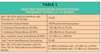

Table 2
The data in Tables 1 and 2 is based on the use of very robust input stages necessary to enable operation in a highly contested environment. These input stages use filters and amplifiers in a cascaded configuration where some elements can be bypassed. Consequently, the total receiver noise figure (NF) with all filters active is on the order of 10 dB, typically 4 to 6 dB higher than usually expected. In situations where no strong interferers are present, some co-site filters can be bypassed and additional high gain amplifiers can be activated, which leads to noise factors on the order of 4 dB or less.1
WHAT ABOUT RECEIVER INTERMODULATION?
The specifications in Tables 1 and 2 do not show values for receiver intermodulation because in a co-located environment, all interferers that may cause intermodulation products within receiver front-ends are those radiated from transmitters at the same station. These transmitted signals are present at any other transmitter antenna and create so-called backward intermodulation products, which are then reradiated into the station.
These spurious signals appear at the same frequencies where receiver intermodulation signals would appear as well. This means that even with no receiver intermodulation effects at all within a radio station, operation on a frequency affected by transmitter backward intermodulation is not possible.
The designer of a receiver front-end can set the intermodulation performance of the front-end to reasonable values by hiding the expected receiver intermodulation products behind those generated by the transmitters. Consequently, the operational system limit of the radio station is not limited anymore by the receiver intermodulation performance, but by cross-modulation.
Cross-modulation is a critical effect in communication systems with waveform amplitude changes or amplitude modulation (AM). This is the case, for example, in systems used for air traffic control because the communication waveform used is a double-sideband AM signal.
Cross-modulation occurs when a strong interferer drives the front-end into saturation. If an amplifier is saturated, its gain is reduced and any other low-level signal passing through the amplifier at the same time also sees some reduction of gain. As a result, the low-level signal is inversely modulated by those parts of the interferer’s envelope that saturate the front-end.
An air traffic controller operating on a voice channel cross-modulated by another communication channel will not be able to communicate with pilots. Even a very high receive level will not help in this situation. It is therefore essential that all interferers are kept below the cross-modulation threshold of a receiver system to keep it within an area of linear operation. Below this limit, the quality of the reception is determined by key parameters of the receiver and those transmitters acting as interferers.
With additional frequency planning, operation on channels blocked by intermodulation products is avoided and the entire station can operate nearly free of self-created interference.
STARTING WITH THE TRANSMITTER RF CHAIN
The transmitter RF design can be simply seen as an RF signal generator with some following amplifiers that increase the low signal level of the generator to the required high output power at the antenna.
A high-end transmitter is characterized by very low unwanted emissions outside the transmit channel. These unwanted emissions are either discrete signals or are represented by a noise floor. Discrete spurs can be caused by a variety of effects, such as the internal coupling of clock signals into the RF path. Other effects that can create discrete spurs may be based on nonlinearities in the transmit path, mainly within the final power amplifier (PA).
Before the minimization of discrete spurs, the basic transmitter design must first provide a low noise floor; otherwise, the radiated unwanted noise may already significantly interfere with adjacent channels.
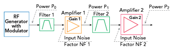
Figure 2 Improved transmitter RF path.
The unwanted noise floor can be divided into two areas, which also represent two different noise-creating mechanisms. Close to the carrier noise is normally called phase noise and far from the carrier noise is called broadband noise. While phase noise is determined by the quality of the RF generator, the broadband noise floor is mainly determined by the design of the amplifier chain after the RF generator.
For a high-end transmitter, the required broadband noise floor might be required to be so low that even with a “no noise RF generator,” the resulting noise floor after the amplifiers may be too high. This means that a significant improvement can only be achieved by inserting filters in the RF path. The optimization of this filter-amplifier chain must then be done by going backward from the antenna through all stages and analyzing the gain of each amplifier stage.
Figure 2 shows a RF path improved by inserting two bandpass filters in front of each of the transmit amplifiers. The minimum broadband noise floor at the output of the transmitter is mainly the noise at the input of Amplifier 2 that is increased by its gain.
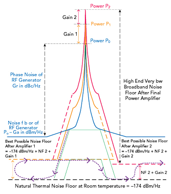
Figure 3 Spectrum of the improved transmitter RF path.
For a first optimization, the elements within the RF path can be seen as ideal, e.g. the filters have no insertion loss and the amplifiers only have a NF plus a flat frequency response with a given gain. It is also assumed that a filter in front of an amplifier completely suppresses all broadband noise coming from previous stages. With this simplification, it is clear that the broadband noise floor after the final amplifier is just the input noise floor represented by the amplifier‘s NF, which is then increased by its gain.
While the output power of the RF generator inside the filters‘ passbands is increased by the amplifiers, the broadband noise floor outside the filters‘ passbands is first suppressed by the filters; then, a following amplifier just increases its input noise floor by its gain. Consequently, the output noise floor always remains quite low while output power increases with the total gain of the transmitter‘s RF path.
In Figure 3, the dotted purple line shows the suppression of broadband noise by the filters, which is then increased by the gain of the following amplifiers. The defining parameters of broadband noise performance are the maximum allowed gains for each amplifier stage, which also define the power levels appearing at all filters.
It may be that the filter in front of the final PA must handle a power level of some Watts due to the quite low allowed maximum gain of the amplifier following it. Such a high-power filter may be difficult to realize, especially because it must be tunable in frequency as well.
On the receiver side, a similar high-power filter may be required to ensure sufficient receiver performance in the presence of strong interferers. Therefore, the dual use of relevant resources like filters and other components for the receive and transmit paths should be considered during the process of optimizing the overall RF transceiver architecture.
The RF Generator (Exciter) is the Heart of the Radio
The most important building block of a transceiver is the RF generator (see Figure 4). It provides a low phase noise modulated RF signal that represents the complete transmit signal of the transceiver. It starts with a sufficiently high level, providing an already low broadband noise as a starting point to the following filter/amplifier chain of the transmit path. In receive, the unmodulated RF signal is either used as a local oscillator for superheterodyne receivers or is used as a clock signal for digital direct sampling receivers.1
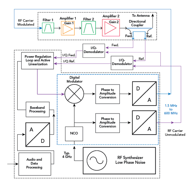
Figure 4 Transceiver RF generator.
Today it is technologically possible to realize the core part of the RF generator, represented by the box with the blue dotted lines in Figure 4, with a fully integrated solution. Even digital-to-analog converters (DACs) can be part of such a chip. Only some manufacturers currently provide fully integrated solutions, but with a split between purely RF functionality and the core direct digital synthesizer (DDS), a sufficiently higher number of components is available.
The information signal (e.g., voice or data) to be transmitted is filtered and adjusted in level and is then digitized. The digitized signal passes through a baseband processing stage that creates a digital I/Q signal stream representing the modulation, including filtering. This digital I/Q modulation information is complex multiplied with the digital unmodulated carrier signal from the numerically controlled oscillator (NCO). This fully I/Q modulated digital RF signal is then input to a DAC and appears at its output as an analog RF signal to be transmitted.
Smart Power Control Loop
It is recommended to use a configuration for the RF generator where two parallel outputs are available, one with the modulated RF transmit signal, and one with the same, but still unmodulated, RF signal, derived from the same digital oscillator. This second unmodulated signal can be used to supply two feedback paths that provide phase-coherent demodulation of the RF signals present at the directional coupler after the final PA.
The signal from the forward output of the directional coupler can be used to set up a power regulation loop by monitoring the level of the transmit signal. This feedback signal can also be digitally compared with the transmitted signal to identify any signal distortions. A so-called active linearization loop is now able to pre-distort the transmit signal, compensating for all influences which happen on the way to the antenna through all stages.
The second feedback demodulator is connected to the reflected output of the same directional coupler and allows a highly capable analysis of all signals traveling from the antenna back to the final amplifier.
Due to the phase-coherent nature of the demodulation, it is now easy to distinguish between signals that are reflections of the transmit signal and those that have been radiated backward into the transmit antenna by other transmitters. Signals from other transmitters are characterized by a frequency offset when compared with the transmitted signal and can now be isolated. This enables an optimized strategy, keeping the transmit power constant or reducing it not any more than necessary, independent of the source of the reflected signals.2
Always Design the PA for Good Linearity
The active linearization capability shown in Figure 4 is a regulation loop that can reduce the effects of nonlinearities from all elements between the RF generator and the antenna. It must be carefully designed with respect to its bandwidth; otherwise, it may increase the noise outside its bandwidth where broadband noise begins. Even with this capability in a transmit path, any amplifier should always be designed to provide good linearity.
Nonlinearities of amplifiers can be based on a variety of mechanisms and are often described with very complex formulas, but the practical view is much simpler. If, for example, a digitally modulated single carrier is used as a transmit signal, then linearity is just how fast and how accurately the output signal of an amplifier can follow the input signal in phase and amplitude.
The AM frequency response of an amplifier is a major parameter in the context of nonlinearities, and this AM frequency response is set and limited in most of the cases by the circuitry of the input stages, not by the transistor. For a Class AB amplifier, the gate voltage may increase with an increasing RF drive signal, which opens the transistor for a higher output power. This leads to a dynamic shift of bias voltage toward Class A. It is important that the average DC bias voltage at the gates follow the average level of the drive signal fast enough; otherwise, the output power of the transistor cannot follow amplitude changes at the input fast enough. Figure 5 shows a simplified schematic of a push-pull amplifier, which may limit its AM frequency response.
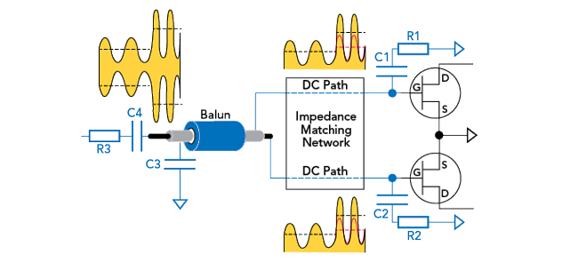
Figure 5 Input circuit limiting AM frequency response.
The incoming RF signal is changed from unsymmetric to symmetric by the balanced-to-unbalanced (BALUN) circuit. Relative to GND, one transistor is driven with the positive half of the RF carrier sinewave, while the second transistor is driven with the negative half, and vice versa.
The envelope of the modulation signal represents the level of the RF carrier and should look identical on both gates. The average instantaneous level of the envelope is responsible for opening the gate to the required source gate voltage (shown as dotted lines in Figure 5).
The elements C1/C2 and R1/R2 set a lowpass characteristic. If the time constants are set too low, then the average DC voltage of fast modulation peaks cannot follow these fast changes in the envelope. Consequently, the gates are supplied with gate voltages that are too low (shown as red dotted lines) during fast modulation periods while the RF envelope is reaching full amplitude.
This leads to the suppression of fast amplitude signal changes, which looks like amplifier saturation. This mechanism creates almost the same intermodulation distortion as a saturated amplifier, but it is simply caused by a bandwidth limitation of the DC paths within the input circuits of the PA.
It is therefore recommended to first optimize the AM frequency response of a PA according to the required bandwidth of the transmitted signal and use the feedback loop only for further optimization of the remaining nonlinear behavior, if necessary.
It is a good choice to design an amplifier for an AM/FM frequency bandwidth response that is at least 2x or 3x higher than the highest modulation frequency of the signal to be transmitted. For an HF amplifier operating an SSB Voice signal, the AM frequency response shall be at least at 6 to 9 kHz. This method of improving amplifier linearity is easy to achieve and is easily validated because only an AM-modulated signal is required for testing.
In a push-pull configuration, it is also important that the gates of both transistors see identical circuits. Within Figure 5, a DC path through the matching network connects the gates to both capacitors C3 and C4. These capacitors likely have different values because they have been selected based on different goals. Additionally, C4 is connected to a series impedance, while C3 is directly connected to GND. As a result, AM frequency responses at the two gates may be different due to different capacitive loads, which leads to unequal transistor drives.
With a good design for the PA in combination with linearization, the following two-tone intermodulation values can be expected if the transmitter is driven with a two-tone signal level 6 dB below peak envelop power for each tone. The IM3 values represent the difference between the intermodulation products and the two tones:
- IM3 ≥ 30 dB – basic linearity
- IM3 ≥ 40 dB – enhanced linearity using digital predistortion
- IM3 ≥ 45 dB – superior linearity using digital active linearization.
On the receive side, an HF receiver (whether using direct sampling or intermediate frequency (IF) sampling) may be used as an IF receiver after a VHF/UHF down-converter as part of an overall superheterodyne concept.
Splitting into sub-bands makes sense for components close to the antenna. However, for an RF generator, it is possible today to create highly linear signals with low phase noise up to very high frequencies, where a split into sub-bands does not provide any advantage.
CONCLUSION
A transceiver architecture comprises circuits for transmit and receive that can be completely independent of each other. An important step in optimization, however, is to harmonize key parameters of the transmit path with those of the receive path for best system performance where these functions are co-located with low antenna decoupling.
It should be a goal for the designer that the robustness of the receiver is matched to the noise performance of the transmitter with a given antenna decoupling. The harmonization of the receive path with the transmit path within a transceiver architecture is then the basis for sharing valuable resources.
Figure 6 High-end configurable V/UHF software-defined radio (SDR).
These shared resources may be high-quality filters that act as pre-selectors for the receive path or as co-site filters to reduce the noise of the transmit path. Another sharable resource is a low noise signal generator providing a clean signal in transmit that is also used as a clean sampling or mixing signal in receive for best desensitization performance.1
For high-end installations, such as military communication sites, radios can be adapted to the co-site situation (see Figure 6). These radios can be equipped with special co-site options like hopping filters. Co-site filters are not only used as pre-selectors for enhanced receiver robustness, but they are also re-used as bandpass filters within the transmit chain.
The co-site filters are active in all operational modes including fast frequency hopping modes, ensuring a highly robust communication link, even in the presence of intentional jamming. The RF specifications enable interference-free operation in complex antenna systems with antenna decoupling values as low as 25 dB.
Transmitters can additionally be equipped with optional circulators to reduce transmitter backward intermodulation effects and, in combination with a frequency planning, spurious-free operation can be achieved.
ACKNOWLEDGMENT
We thank Ludger Korsmeier, Manfred Fleischmann, Robert Traeger and Harald Wickenhäuser DK1OP (all Rohde & Schwarz) for their support during the creation of this article.
References
- U. L. Rohde and T. Boegl, “The Perfect HF Receiver. What would it Look Like Today?” Microwave Journal, Vol. 65, No. 5, May 2022, pp. 68–82.
- H. L. Hartnagel, R. Quay, U. L. Rohde and M. Rudolph, Fundamentals of RF and Microwave Techniques and Technologies, Chapter 9.6, Springer, 2023.
For Further Reading