
Software-Defined Direct RF Simultaneous Sampling Multi-Band/Service Transceiver
Microwave RF transceiver system development (L- through Ka-Band) is rapidly changing as new hardware becomes available. Significant advances in analog-to-digital converters (ADCs), digital-to-analog converters (DACs), system on chip (SoC) and system in package (SiP) technologies, requiring varying degrees of corresponding software, create a daunting set of variables for today’s engineers.2 In addition, expanding market applications requiring simultaneous processing of multiple microwave RF bands to provide multiple services, such as ground penetrating radar, navigation and satcom, while adhering to SWaP-C constraints, requires next-generation planning and partnering. Newly developed L- through Ka-Band ADCs, DACs and mixed signal systems in packages (MiXiP SiPs), including SoC field-programmable gate arrays (FPGAs), solve these problems.1 They are completely software controlled, enabling simultaneous sampling for multi-band and multi-service operations.

Figure 1 Conceptual difference between heterodyne and homodyne transceivers.
RF transceivers have traditionally employed a heterodyne architecture (see Figure 1). A transmitted (Tx) or received (Rx) analog RF signal is derived from a DAC or digitized by an ADC through a mixer (up-converted for Tx or down-converted for Rx) with a local oscillator (LO). The derived Tx and Rx signals are “In-Direct” to the RF and are called the intermediate frequency (IF) signals.
IF signals (Tx or Rx) are the sum or difference of the RF and LO signals (RF = IF + LO or IF = RF - LO).
The heterodyne architecture is generally designed for a single frequency band and single service. The advantages of the heterodyne architecture are low-cost, mature implementations, available narrowband components and hardware switchable reconfigurations. The disadvantages are that it is hardware constrained, single band (narrow), single service and limited to sequential sampling/operations.
Some microwave RF transceivers use a homodyne direct RF architecture (see Figure 1).5 Direct RF eliminates the need for mixing (or up/down frequency conversion) and processes the Tx and Rx signals directly in the appropriate RF band required for the service operation. Effectively, direct RF looks like a wire between the antenna from the DAC/Tx or to the ADC/Rx.
The evolution from heterodyne to homodyne transceiver development enabled by advancements in both hardware and software, is shown in Figure 2. Over this time, the greater the processing bandwidth of the hardware, along with software development, has incrementally reduced transceiver analog hardware to the point that the transceiver simply becomes a software-defined radio.

Figure 2 Evolution to software defined radio from L- to Ka-Band.
Teledyne e2v now offers a direct RF simultaneous sampling multi-band/service transceiver for conversion up to Ka-Band.1 This single chain transceiver can convert L- through Ka-Band simultaneously (not sequentially) for multi-service operations. This direct RF conversion approach requires that the Tx/Rx module be as close to the antenna as possible, along with all the required circuitry for digital frequency conversion, beam steering, modulation and demodulation functions.
Optimal noise and frequency performance is realized without up-/down-conversion and insertion losses are reduced with no combiner/splitters required. For frequency planning, once the hardware implementation is set (e.g., data converters and filters), the only design variable in the system (other than software reconfigurations) is the sample clock frequency. A completely software-defined system allows for continuous dynamic software reconfigurations, ultimately using AI technology.
TRANSCEIVER APPLICATIONS AND IMPLEMENTATIONS
Microwave transceivers include both Tx and Rx functions within the same module using either heterodyne or homodyne architectures. Transceivers either operate in half-duplex or full-duplex modes. Half-duplex means that Tx and Rx functions must alternate in time, while full-duplex allows the system to transmit and receive data simultaneously.
Figure 3 shows various satellite applications operating in different RF bands.3 Traditionally, transceivers were designed as separate systems per application per RF band. This resulted in one investment per single band per service (for Figure 3, this could represent 19 individual investments and developments/deployments). To maximize functionality (multi-band and multi-service) and minimize development costs, switchable transceiver channels can sequentially switch analog and digital channel functionality with delay times in-between.

Figure 3 Individual transceiver development per service and band.
Today’s direct RF transceiver developments are efficiently designed for multi-band performance per service (see Figure 4). Unfortunately, multi-band operation may be limited, such as L- and C- or X- and Ku-Bands, depending on the ADCs and DACs that are available. Whether multi-service operation can be fully realized generally depends on digital modulator/demodulator processing and computation speeds. Digital data routing can also be a significant impediment.

Figure 4 Advanced FPGA devices (a) allow unprecedented signal processing capabilities, enabling waveform management of multiple services simultaneously from one system/one investment (b).
Enabling waveform management of multiple services simultaneously as shown in Figure 4 is accomplished with this new direct RF simultaneous sampling multi-band/service transceiver. It simultaneously (not sequentially) processes multiple bands (L- through Ka-Band) as well as multiple services. This is accomplished using Teledyne e2v’s Ka-Band capable ADCs and DACs in conjunction with AMD Xilinx’s advanced 7 nm FPGA XQRVC1902 digital engine packaged together using MiXiP SiP technology.
A multi-band/service microwave transceiver, besides requiring ultra-high performance components, requires cutting edge packaging and interconnect technology to partition the system in ways that minimize analog and digital interference.2 Figure 5 shows several transceiver partitioning techniques: 1) common single multi-chip module with centralized data around the FPGA that minimizes digital routing, 2) SoC and 3) SiPs interconnected with optical digital fiber that place the ADCs and DACs near the antenna while isolating the digital functions from the analog.

Figure 5 Transceiver Partitioning: MCM (a), SoC (b), SiPs + SoC (c).
Technique 1 has been used for decades but requires complex routing of analog signals for both the ADCs and DACs. Of course, as operational system frequencies increase, analog signal routing becomes problematic.
Technique 2 uses an SoC, which requires monolithic process technology and device geometries that must accomplish both the microwave analog and digital functions necessary for the transceiver. This is very difficult, expensive and requires extreme development timeframes.
Technique 3 combines the best of both techniques 1 and 2 but requires optical data link drive capabilities and is not offered by Teledyne e2v. It lends itself particularly to the use of separate transmitters and receivers connected to separate antennas.
DIRECT RF SIMULTANEOUS SAMPLING MULTI-BAND/SERVICE TRANSCEIVER ARCHITECTURE
Figure 6 is the block diagram of a software-defined direct RF simultaneous sampling transceiver in a single, contained, transceiver antenna module (TAM) connected directly to the antennas for L- through Ka-Band service/operations. At the core of the TAM is the Tx/Rx MiXiP SiP which houses Teledyne e2v’s EV12DD700 (DAC), two EV10AS940 (ADCs) and AMD Xilinx’s XQRVC1902 7 nm FPGA digital engine. The TAM also includes auxiliary components such as lowpass filters (LPFs), bandpass filters/multi-band (n) pass filters (BPFns), low noise amplifiers (LNAs), high-power amplifiers (HPAs) and circulators.1,2,5

Figure 6 Software-defined direct RF simultaneous sampling transceiver.
Packaging and partitioning of the TAM depends on the required service frequency bands, power transmission levels, physical dimensions and thermal requirements of each auxiliary component. For example, it may be optimal to have the MiXiP SiP, LNAs, LPFs and BPFns on a single PCB directly connected to the HPAs and circulators, which would in-turn connect to the antennas.
The advantages of a TAM that uses the L- through Ka-Band operational MiXiP SiP core is that the system is no longer hardware constrained. With the DAC, ADCs and FPGA MiXiP SiP’s ability to operate up to Ka-Band and with the system contained within a single SiP package, developers need only select from a vast array of auxiliary components to meet system performance requirements.
Once the auxiliary components are selected, the TAM becomes completely software-defined (dynamically software reconfigurable) with simultaneous sampling, handovers and seamless connectivity. Once the TAM hardware implementation is set, the only design variable in the system (besides software reconfigurations) is the sample clock frequency. The simultaneous sampling multi-band and multi-service operational capabilities of the TAM provide users with greater system-level resilience, independence of local/terrestrial/space EM infrastructures and automatic switching, which also enables other functions such as system monitoring, encryption operations and antenna blockage avoidance.3
Transmitter DAC
The EV12DD700 is a Ka-Band capable, radiation-tolerant, dual current-steering, 12-bit DAC with conversion rates up to 12 GSps. It can synthesize signals at frequencies over 21 GHz without up-conversion (see Figure 7). It embeds digital features like interpolation, digital up-conversion, direct digital synthesis, chirp, beamforming, beam hopping and ultra-fast frequency hopping.1,2,8

Figure 7 EV12DD700 (a) and amplitude versus output frequency (b).
The sinc(x) = sin(x)/x DAC output response can be compensated through the anti-sinc feature (A-SINC). In addition to the classical non-return-to-zero output mode (NRZ), the DAC cores have an embedded RF mode and a 2RF mode requiring a clock at twice the speed of other modes. These output modes enable the DAC to directly synthetize frequencies up to 21+ GHz without an external up-converter for operation up to and including Ka-Band.
Figure 8 shows the spectral output of the device when simultaneously transmitting L- and C-Bands (DAC Channel A (NRZ mode)) and X- and Ku-Bands (DAC Channel B (RF mode)) output signals.
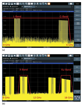
Figure 8 EV12DD700 simultaneous output: L- and C-Bands (a), X- and Ku-Bands (b).
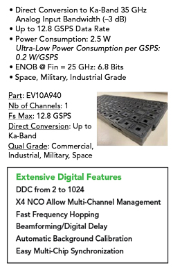
Figure 9 EV10AS940 performance and features.
Receiver ADC
The EV10AS940 is a 10-bit Ka-Band capable single channel ADC enabling sample rates up to 12.8 GSps. It also features digital down-conversion (DDC) and frequency hopping (FH) capabilities with multiple digital channels by integration of multiple numerically controlled oscillators. Other extensive digital features are included as well (see Figure 9).
Its high analog input bandwidth (35 GHz) makes it the best choice for direct RF Ka-Band architectures, eliminating any requirements to integrate dedicated mixers. Power consumption is as low as 2.5 W. It also features 11 ESIstream serial links that operate synchronously with the sampling clock to achieve deterministic data transfer.
DDC functionality has multiple options for decimation rates with up to four independent NCOs to support FH in multi-band operation. Coherent FH is possible due to multiple phase accumulators on each NCO and deterministic dedicated hopping trigger I/Os. Digital integer and fractional delays enable beamforming for use in phased array applications.
Other features include background and temperature calibration, temperature monitoring, DDC with decimation ratios from 2 to 1024, 4 DDC channels, dedicated FH I/Os, deterministic FH with return to zero, continuous and coherent modes, ESIstream 62/64b, high speed serial link (HSSL) reach selection and HSSL impedance control (2 × 50 Ω ± 20 percent).
Table 1 shows spurious free dynamic range (SFDR) and Table 2 shows noise power ratio (NPR), which are helpful in assessing the ADC’s multi-band/multi-tone performance capabilities.

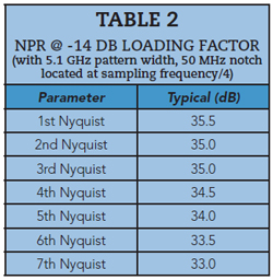

Figure 10 Tx/Rx MiXiP SiP core for a TAM design.
Figure 10 shows the Tx/Rx MiXiP SiP core of the TAM which houses the EV12DD700, 2 EV10AS940s and the XQRVC1902. The complete MiXiP SiP transceiver has a compact form factor outline of 63 × 50 mm with a SiP ball matrix of 52 × 47 mm. The SiP (substrate patent pending) is pre-built using rad-tolerant DAC and ADCs with known reliability.
The ADCs also have single-ended inputs which are extremely helpful when selecting LNA drivers and eliminating the need for any transformer/balun requirements. Of course, the MiXiP positions the XQRVC1902 are next to the DAC and ADCs, thereby minimizing digital routing and reducing interference.
The AMD Xilinx VC1902 (7 nm) is a Versal-based AI core and adapt compute acceleration platform (ACAP) AI inference engine. Versal AI cores offer breakthrough AI inference that deliver over 100x greater performance than server-class CPUs.
The Versal ACAP is a comprehensive SoC that combines CPUs, DSPs, I/O and RAM control along with programmable hardware logic. The XQRVC1902 enables the Tx/Rx MiXiP SiP to have dynamic frequency planning and to be software controllable, flexible, multi-band, multi-service and able to crossband (receive multiple bands while simultaneously transmitting other bands).
TAM Auxiliary Components
To fully implement a software-defined direct RF simultaneous sampling multi-band/service transceiver operating from L- through Ka-Band, each system component is a key enabler. Besides using the Ka-Band capable Tx/Rx MiXiP, every other system component must be evaluated and understood from a simultaneous sampling multi-band performance perspective as well.6,7
For example, six simultaneous Tx/Rx RF bands/tones will be processed by the antennas, HPAs, LNAs, filters and circulators. Traditionally, these components are evaluated by varying single tones and/or two-tone tests. What is required now, however, is a multi-band performance evaluation mindset for each component.
This is where NPR testing might prove useful. NPR testing is typically thought of in terms of the “quietness” of a specific band within a multi-band system. Noise and intermodulation distortion products of other bands will fall into a specific band. Therefore, NPR testing may prove helpful in assessing auxiliary components’ multi-band/multi-tone performance capabilities. Some considerations for selecting TAM auxiliary components are:
Antennas and Operating Frequencies/Polarizations
If all Tx and Rx signals are in same plane, use linear polarized antennas; if not, use circular polarization. Wideband (circular polarized) antennas are generally provided by defense/satcom suppliers and a few commercial suppliers.
Wideband antenna design requires tradeoffs between antenna gain, antenna size, multi-beam capability, beamforming/shaping and steerability. Note that Ka-Band bandwidths are 4× larger than lower bands and therefore use multiple focused spot beams for frequency reuse operations that allow for Tx/Rx of different signals simultaneously at the same frequency.4
Ka-Band is susceptible to adverse weather conditions and therefore requires alternate/additional bands for seamless operation. It also has a greater number of orbital slots and capability for high capacity/density with smaller steerable beams. Ka-Band is resilient, using high data rates without degradation on smaller terminals and employs smaller antenna sizes than other bands (approximately ¼ size).

Figure 11 EV12DD700 SFDR vs. frequency.

Figure 12 EV12DD700 phase noise.

Figure 13 EV10AS940 SFDR vs. frequency.
HPA
The HPA converts low-power RF signals (from the DAC) into high-power signals that drive the transmit antenna. Required specifications include gain, power output, output drive configuration (e.g., Class A, AB), bandwidth, efficiency, linearity (low signal compression at rated output), input/output impedance matching and heat dissipation. Each HPA component must be evaluated and understood from a multi-band simultaneous sampling performance perspective (as previously noted).
LNA
The LNA converts and amplifies very low-power RF signals from the antenna without significantly degrading signal to noise ratio and drives the receiver ADC. Required specifications include gain, noise figure, bandwidth, linearity, gain flatness, stability, input/output impedance matching and maximum RF input. An RF LNA must be low noise, high gain and have a sufficiently large intermodulation compression point (IP3 and P1db). An RF LNA must be protected by a power limiter to recover from large input signal transients that can occur during duplex switching (from Tx to Rx transitions).
Circulators/Switches (Duplexers)
RF duplexers enable bidirectional signal transmission through a single path (isolating the receiver from the transmitter and permitting them to share the same antenna). RF circulators enable full-duplex transceiver operations (transmitting and receiving at the same time with a single shared antenna over various frequencies). Ports are connected through waveguide transmission lines as well as microstrip line or coaxial cables. Specifications include frequency range, insertion loss, return loss, isolation, rotation and maximum power handling.
Waveguides/Filters
Waveguides are hollow metal pipes used as transmission lines connecting the transmitter and receiver to the antenna and the geometry of the waveguide structure can also serve as a filter to determine which frequencies are passed and which are rejected.
Clock Generator
The clock generator is an electronic oscillator that produces clock signals for use in synchronizing system-level operations. The clock generator must be programmable and provide enough drive for multiple copies to be distributed throughout the system. Specifications include frequency range, programmability, power drive, phase noise and jitter.
Optical Digital Harness
An optional optical digital harness may also be useful. It electrically isolates the system interconnections and enables further antenna digitization and weight reduction.
MEASURED PERFORMANCE
Figures 11 and 12 show SFDR and phase noise performance of the EV12DD700 DAC.
Figures 13 and 14 show SFDR and uncalibrated/calibrated performance of the EV10AS940 ADC.

Figure 14 EV10AS940 frequency performance uncalibrated (a) vs. calibrated (b).
CONCLUSION
Microwave RF transceiver developers face design challenges for simultaneous sampling, multi-band and multi-service systems while adhering to SWaP-C constraints. In addition, the continuous release of next-generation ADCs, DACs and FPGAs impact hardware development plans driving frequent redesign.
Now, however, Tx and Rx data conversion components can achieve L- through Ka-Band capabilities and advanced SiP assembly technologies place the FPGA within the same package. These advances enable Teledyne e2v’s Tx/Rx MiXiP SiP design for microwave RF transceiver systems with software-defined flexibility and multi-band/multi-service capability. Teledyne e2v’s advanced MixSiP SiP design gives TAM designers the highest performance (up to Ka-Band) and value through a software-defined direct RF simultaneous sampling multi-band/multi-service transceiver.
References
- S. Lischi, R. Massini, R. Pilard, D. Stagliano and N. Chantier, “Feasibility Study of a Fully-Digital Multi-Band SAR System operating at L, C, X and Ku Bands,” 7th Workshop on RF and Microwave Systems, Instruments & Sub-systems + 5th Ka-band Workshop, May 2022.
- F. Deviere, N. Seller and J. Rohou, “Making History: Advanced System in a Package Technologies Enable Direct RF Conversion,” White Paper, Microwave Journal, Vol. 64, No. 1, January 2021.
- B. Dunbar and S. Caldwell, “9.0 Communications,” National Aeronautics and Space Administration, March 2022.
- R. Cohen-Hirsch, “Why Ka-Band Best Supports the Modern Miliary Mission,” MilsatMagazine, September 2015.
- T. O’Farrell, R. Singh, Q. Bai, K. L. Ford, R. Langley, M. Beach, E. Arabi, C. Gamlath and K. A. Morris, “Tunable, Concurrent Multi-band, Single Chain Radio Architecture for Low Energy 5G-Rans,” IEEE 85th Vehicular Technology Conference (VTC Spring), June 2017.
- S. Amin, P. Handel and D. Ronnow, “Characterization and Modeling of RF Amplifiers with Multiple Input Signals,” Conference: Swedish Microwave Days, March 2016.
- X. Yang, S. Li and F. Li, “Fourth-Order Nonlinear Distortion to the Power Spectrum of RF Amplifiers,” The Journal of Engineering: The Institute of Engineering and Technology, Vol. 2022, No. 1, January 2022, pp. 53–63.
- A. Patyuchenko, M. Younis, S. Huber, F. Bordoni and G. Krieger, “Design Aspects and Performance Estimation of the Reflector Based Digital Beam-Forming SAR System,” Conference: International Radar Symposium (IRS), April 2009.