

Online Spotlight: Balun Measurements with a Two-Port Vector Network Analyzer
The measurement of balanced devices uses a two-port vector network analyzer (VNA) and a pair of baluns. A method for de-embedding the baluns using the built-in de-embedding feature of the VNA is described.
Balanced measurements are necessary for many applications. High speed digital transmission lines are often employed on printed circuit boards to transport signals with extremely high bandwidths. It is important to be able to verify insertion loss, characteristic impedance, phase imbalance and cross talk to adjacent conductors. Antennas are sometimes fed with balanced lines as well, and being able to verify the return loss or VSWR of the balanced feed plus antenna combination is useful.
USING A VNA FOR BALANCED CHARACTERIZATION
A vector network analyzer makes only unbalanced measurements. That is, each port sends and receives signals on a coaxial cable where the RF excitation signal and any reflections progress on the center conductor and the equal and opposite return signal is carried on the inside of the coaxial shield (see Figure 1). No RF current should flow on the outside of the shield.

Figure 1 Coaxial RF current flow.
As a side note, we rarely think about the return path on the inside of the shield. Consider that there is no net magnetic field generated by the cable since the two signals have opposing fields and cancel. Therefore, it is possible to clamp a ferrite core on the outside of the cable to prevent externally induced RF from traveling on the outside of the shield. If the two currents did not cancel, the ferrite would make the center conductor unacceptably inductive, but because they do, there is no net effect on internal signal propagation.
Because the VNA does not generate a balanced drive signal, it is necessary to use two ports to measure a balanced input or output. For example, in Figure 2, one side, “A,” of the input is driven by port 1, while port 2 maintains a 50 Ω termination on side “B.” “B” is then driven by port 2 and “A” is terminated by port 1. The two unbalanced measurements may be combined to calculate the effective balanced response. It is important to note that this method only works with a passive, linear device under test (DUT). An active differential device may not exhibit linear behavior if only one input is driven at a time. In that case, the linear combination of one driven input with the other port terminated will not likely be the same as the case where both inputs are driven simultaneously with a balanced drive.

Figure 2 Measuring a balanced input.
For a differential measurement, the A/B terminals of the DUT are called differential port 1. This can be confusing, but differential port 1 S-parameters are derived from the unbalanced measurements from VNA ports 1 and 2.
For example, the calculation for the input Differential S-parameter of the DUT in Figure 2 is:

(The 11 subscript on SDD refers to the A/B differential port 1, not port 1 of the VNA) The differential input looks like the sum of the two-port reflections A and B minus the two cross terms between them.
The two-port VNA software, “S2VNA” from Copper Mountain Technologies does not have this measurement conversion built-in, but data can easily be taken using standard commands for programmable instruments (SCPI) and processed to produce differential S-parameters.
As a further example, the differential “insertion loss”1 through the differential device, or SDD21, requires a 4-port measurement (see Figure 3). Differential return loss is found by Equation (1) and insertion loss is:

With appropriate unbalanced measurements, it is, therefore, possible to determine balanced performance.

Figure 3 Full balanced measurement of a DUT.
BALUN TYPES
There are two types of baluns: voltage and current (see Figure 4). A voltage balun forces the balanced output to have equal and opposite voltages. The two currents are not necessarily balanced. A current balun forces the balanced output currents to be equal and opposite2.

Figure 4 Balun types: voltage and current.
The voltage balun generates balanced voltage outputs, acting as a transformer. It will not operate well at low frequencies where coupling is reduced and resonance with interwinding capacitance limits its high frequency response. The current balun can generally operate over a wider bandwidth and produces a balanced output current by virtue of magnetic coupling presenting a high impedance to unbalanced currents. At low frequencies, the signal may pass through the chokes, but common-mode rejection will be poor. Resonance at high frequencies is also an issue. There are a great number of balun types and configurations, but the focus here is the characterization of a balun for use with a two-port VNA.
BALUN CHARACTERIZATION
A Balun, which is a contraction of the words balanced and unbalanced may be attached to a VNA port to convert the unbalanced port for a balanced measurement. With two baluns, a two-port VNA can make fully balanced measurements of passive or active devices. For accurate measurements, the baluns must be fully characterized, and their effects removed (de-embedded) from the measurement to ascertain the response of the DUT alone.
Before proceeding, it is important to understand the mixed mode S-parameter measurements which apply to a balun. A balun has a single-ended (SE) port on one side and balanced (Bal) port on the other.

Figure 5 Balun ports.
Port 2 in Figure 5 has two components. One component is the balanced signal where the phase difference is precisely 180 degrees between the two connections of the port. The other component is the common-mode signal where the phase is zero degrees between the two connections. A perfect balun creates only a balanced signal on port 2 if excited by a signal on port 1. No common-mode (in phase) signal is generated.
No balun is perfect, however, and there is always a combination of both. Note that any small phase shift introduced on either of the differential outputs will create a small common-mode component on that port, an effect particularly noticeable at higher frequencies. Proper PC layout with trace length matching is therefore important for the printed circuit board layout of a surface-mount balun. Mixed mode parameters for a balun are defined in Table 1.

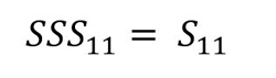
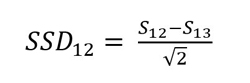
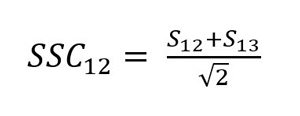
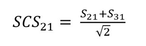
These mixed mode parameters define all differential and common-mode effects of the balun:
SSS11 is the return loss looking into the SE Port 1.
SSD12 is the SE signal developed on Port 1 from the balanced signal on port 2.
SSC12 is the SE signal developed on port 1 by the common-mode signal on port 2. This should be a very small number for a good balun.
SDS21 is the differential “thru” response of the balun.
SDD22 is the differential port 2 return loss.
SDC22 is the differential mode reflection from Port 2 due to a common-mode excitation.
SCS21 is the common-mode signal generated on port 2 by the SE port 1 input. This should be very small for a good balun.
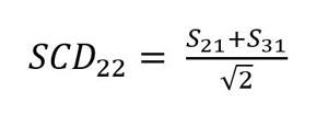
SCD22 is the common-mode reflection from Port 2 due to a differential mode excitation.
SCC22 is the common-mode reflection from Port 2 due to a common-mode excitation.
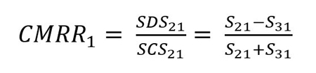
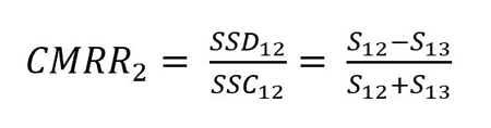
Additional figures of merit for a balun are its common-mode rejection ratios in each direction:
CMRR1 = SDS21/SCS21, the ratio of the differential to common-mode signal generated on Port 2 by a signal on Port 1
CMRR2 = SSD12/SSC12, the ratio of the SE signal generated on Port 1 by a differential signal on Port 2 to the one created by a SE signal on port 2.
Both common-mode rejection ratios should be reasonably large numbers for a good balun. A ratio of 10 or more (linear magnitude) is reasonable.
All mixed mode characteristics may be calculated from a three-port measurement of the device.
MIXED MODE PARAMETER CALCULATION FROM UNBALANCED VNA MEASUREMENTS
For measurement, the balun is connected to the VNA as shown in Figure 6. The diagram depicts a voltage balun, but the configuration is unimportant. It is simply assumed that port 1 goes to the unbalanced Logical Port 1, and ports 2 and 3 are attached to balanced Logical Port 2.

Figure 6 Balun connections.
In the following formulas, port numbers 1, 2, and 3 are used for the VNA S-parameter subscripts and the mixed mode S-parameters like SDD22 are designated by logical ports 1 and 2. A full 3-port measurement of the balun is required, but this could be performed two ports at a time with a two-port VNA while terminating unused ports with a 50 Ω load. The mixed mode S-parameters are calculated as follows:3


DE-EMBEDDING
Under normal circumstances, if an adapter is added to a VNA port, one could measure its two-port response and then use de-embedding to remove its effect on the measurements. De-Embedding is a standard feature on Copper Mountain Technologies’ VNAs and is accessed under the “Analysis” menu. A balun is not a two-port device, however, so in this case, the standard method is not possible; but an approximate method does exist.
SDS21 is like S21, SSD12 is like S12 and SDD22 is somewhat like S22. If a two-port matrix is formed from these values and then used for de-embedding, the results are reasonable. To be clear, a normal two-port S-parameter matrix measurement of an adapter would be used but the differential equivalent may be substituted as an approximation. A normal S-parameter matrix for de-embedding:

Differential Approximation:

The reason why this method is only approximate is that the balun is not perfect and SCS21 of the first balun in a pair used for measuring a balanced DUT is not zero. A small common-mode signal is created on the output of this balun along with the balanced signal. This signal is passed along and creates a small, unbalanced signal on the output balun due to its SSC12. This signal adds to that created by SSD12. These balun imperfections result in small errors in the de-embedding. A more thorough treatment using all mixed mode parameters is certainly possible, but this must done with post-processing in Python or some other programming language while the de-embedding matrix (15) can be used with the built-in de-embedding feature of the VNA.
It is possible that the DUT between the two balun adapters might have a particularly large SCS21 and the small erroneous unbalanced signal created by the balun might be greatly amplified, causing an even larger error in the measurement.
PROTOTYPE MEASUREMENT
A pair of baluns is evaluated, and de-embedding files are created. The ADC-WB-BB baluns from Texas Instruments are made from Mini-Circuits TC-1-13MA+ baluns mounted on connectorized circuit boards (see Figure 7). The frequency range is 4.5 MHz to 3 GHz.

Figure 7 Balun board.
Three-port S-parameters are measured for the two balun boards over the 4.5 MHz to 3 GHz range and Touchstone de-embedding files are shown in Figure 8 using entries from the de-embedding matrix (15).

Figure 8 Calculated Touchstone file.
The two balun boards are connected back-to-back with a pair of male-to-male SMA adapters (see Figure 9) and measured with and without de-embedding. Figure 10 shows the measured results without de-embedding. Return loss is poor and there is greater than 4.5 dB of loss at 3 GHz.
With de-embedding using the files created for the two baluns, the results are more reasonable (see Figure 11). The return loss is considerably better, and insertion loss is flatter. There are places where the insertion loss is slightly positive, which is clearly an error, but only within a few tenths of a dB. Evaluating the de-embedded baluns in this manner is a good way to estimate the measurement errors.

Figure 9 Balun measurement setup.

Figure 10 Back-to-back baluns without de-embedding.

Figure 11 Back-to-back baluns with de-embedding.
CONCLUSION
The mixed mode S-parameters for a balun are introduced and the method for calculating them explained. A method for creating two-port de-embedding files suitable for use with a 2-port VNA and a pair of baluns is shown and results demonstrated. Errors in the method are examined and for some applications, the convenience of standard two-port de-embedding techniques built into the VNA may outweigh the small errors caused by balun imperfections.
References
- K. Suto and A. Matsui, “Two-Port S-Parameter Measurement of Wide-Band Balun,” Proceedings of the International Symposium on Antennas and Propagation, October 2016.
- R. W. Lewallen (W7EL), “Baluns: What They Do and How They Do It,” ARRL Antenna Compendium, Vol. 1, 1995, pp. 157-164, Web: www.eznec.com/Amateur/Articles/Baluns.pdf.
- “Measurement Techniques for Baluns,” Anaren, May 2005, Web: www.richardsonrfpd.com/docs/rfpd/Anaren_De-embed-BalunTesting_applicationnote.pdf.