
Design Guidelines Using Theory of Characteristic Modes for a Broadband and Broad Beam SIW Cavity-Backed Microstrip Antenna
The performance of a broadband broad beam substrate integrated waveguide (SIW) cavity-backed microstrip antenna (CBMSA) is studied using the theory of characteristic modes (TCM). TCM provides insight into characteristic mode (CM) propagation in the SIW CBMSA, which helps formulate design guidelines for broad bandwidth performance. These guidelines are validated with the design of a 64-element S-Band antenna array. The array is fabricated, and the measurements agree closely with simulation. It demonstrates gain greater than 8 dBi, beamwidth greater than 90 degrees, bandwidth greater than 18 percent, cross-polarization less than -20 dB and efficiency greater than 90 percent. This compares favorably with results reported in the literature.
TCM was first proposed by Garbacz.1,2 Harrington3 formulated it in a matrix form and applied it to scattering problems. It is shown that the CMs are orthogonal and usable as basis functions to represent the induced surface currents on any arbitrary perfect electric conductor (PEC) surface. An electric field integral equation was formulated, relating the surface currents to the tangential electric fields through a Green’s function operator assuming a lossless dielectric.3,4 Now, TCM is applied to numerous electromagnetic problems like antenna design,5-10 antenna beam shaping,5 RCS reduction,11 antenna chassis design12 and antenna-platform interaction.5,13 Antenna bandwidth enhancement is also demonstrated successfully using TCM.6,7,14,15 CMs depend solely upon the shape and the size of an object and are independent of excitation. The feed decides the coupling between the modal excitation coefficients (MEC) and the CMs.5,6 Thus, TCM is useful in designing an antenna with desired characteristics.
Microstrip antennas (MSA) are desirable for the realization of phased array antennas for various applications such as 5G MIMO, phased array radar and direction of arrival (DoA) systems.7,16-18 The U-slot MSA (UMSA) has a broadband capability utilizing multiple resonances,14,15,19-21 and has demonstrated the broadest impedance bandwidth among the family of slotted MSAs.20 In MSA arrays, there is strong mutual coupling (MC) between adjacent structures due to surface wave (SW) propagation.17,22
The CBMSA22,23 has a metallic cavity beneath the MSA that prohibits SW propagation, isolates nearby elements and reduces MC. Thus, it supports the use of a thicker microwave laminate for bandwidth enhancement.16,19 It also enables an overall size reduction: the radiating edge is less than λg/2, where λg is the guide wavelength.22 This increases the -3 dB beamwidth (HPBW) and the separation between nearby elements, assuming λ/2 inter-element separation. This, in turn, reduces MC and avoids the onset of grating lobes (GL).18 Thus, it helps to realize broadband and wide scanning phased array antennas.17,23 The CBMSA, however, is a complicated assembly requiring precise machining of cavities, making it difficult to integrate with multilayer circuit assemblies. The problem is aggravated in larger phased array antennas.
Wu24 introduced SIW technology, which emulates waveguide behavior in a printed form. SIW-based CBMSAs (SIW CBMSA) or slot antennas (SIW-CSA) have been demonstrated.25-35 SIW mimics a metallic cavity with an array of plated through holes (PTH). Thus, it eliminates the need for bulky metallic cavities and exhibits minimal radiation leakage. A broadband SIW CBMSA was proposed for 5G applications.25,43 A C-Band SIW-CSA with HPBW greater than 120 degrees and FBW of approximately 17.7 percent was demonstrated by Wen et al.26 A C-Band CBMSA with a mushroom-like EBG structure by Vilenskiy et al.27 demonstrated a FBW of approximately 12 percent and an 80-degree scan volume. Cai et al.28 demonstrated a multilayer SIW-CBSA operating from 18 to 30 GHz. A wide scan, probe-fed, X-Band SIW CBMPA has also been proposed.28,33 Chou et al.29 describe a SIW-CBSA PAA for DoA estimation. Current literature contains a comprehensive review of SIW antennas.30-35
The design and optimization of SIW-CBMSAs, including probe location, is a time-consuming task using techniques like finite element method, finite difference time domain and method of moments.16 TCM, however, does not require probe inclusion7 and is computationally faster optimizing antenna performance, by providing information on various CMs propagating on the structure. This article describes a strategy for broadband and broad beam SIW CBMSA design using TCM. The CBMSA consists of a U-slot and an annular ring with a PTH array on a thick microwave laminate with low dielectric constant (εr) and dielectric loss (tanδ = td). The annular ring and UMSA have close resonances resulting in broad bandwidth.36,37 The PTH array creates a SIW cavity mitigating SWs, reducing MC and producing a wide scan volume. The antenna’s performance is evaluated in an active array environment. Simulations are compared with the measurements and prior literature.25,27,33,42,43
ANTENNA DESIGN
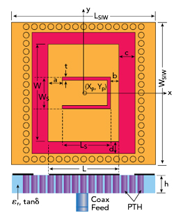
Figure 1 Antenna structure.
The TCM based strategy for SIW CBMSA design with a coaxial probe feed consists of the following design steps (see Figure 1):
- Probe-fed MSA
- U-slot and integration with the MSA
- SIW CBMSA.
The design procedure uses analytical expressions,16 and the TCM module in Altair FEKO software.38 The substrate is Rogers 5880 (εr = 2.2, td = 10-3) with h ∼ 250 mils.
The design objective is an antenna element with broad bandwidth and broad beamwidth for wide scanning phased array applications, meeting the following specifications:
- Frequency of operation: S-Band
- FBW: 20 percent minimum with a center frequency = 3.3 GHz
- HPBW: greater than ±45 degrees
- Low MC and cross-polarization, i.e., less than -18 dB.
Revisiting TCM
CMs are the Eigenmodes forming a basis set for the induced surface currents scattered by PEC bodies.5-7 Thus, the radiation pattern is the linear combination of the respective orthogonal modal currents. The current distribution can be decomposed into mutually orthogonal characteristic currents. The surface currents, J, and scattered electric field, Es, are related through an operator, L, as4

Equation 1 can be re-written for the tangential field component as

In equation 2, the operator part is expressible in terms of impedance as
and

where Z is a complex impedance:

In Equation 5, R and X represent the resistive and reactive portions of the impedance. An eigenvalue (EV) equation is given as:4
In Equation 6, μn are the EVs, and Jn are the eigenfunctions. Using Equations 5 and 6, 7 is obtained in a matrix form as:


Figure 2 Microstrip patch antenna EV (a) and MS (b) vs. frequency; radiation patterns and surface current distributions (c).
In Equation 8, λn is referred to as the EV. Thus, λn = 0 represents the resonance condition, while λn< 0 or λn> 0 represent storage in the form of electric or magnetic energy, respectively. Another characteristic parameter is Modal Significance (MS), which is defined as

MSn→1 represents resonance. Thus, the frequencies satisfying MSn > 0.707, define the FBW of the structure. Another parameter, the characteristic angle (CA) αn, defines the phase angle between the characteristic modal current and respective field and is given in Equation 10:

αn = 180 degrees represents the point of resonance, and its slope gives the FBW. Thus, EV, MS and CA are the essential characteristic parameters that determine the radiation characteristics of the structure and the CMs contributing to radiation. The Eigen currents and the fields are orthogonal; hence, CMs radiate independently of each other and can be used as basic functions to expand the total current (J):
In Equation 11, Vin is the MEC, which assesses the effect of the applied excitations’ position, phase and magnitude on a particular CM’s contribution to the net radiation.
MSA Design
An MSA is modeled (see Figure 2) using simple closed-form expressions16 and analyzed using TCM. All possible mode excitations are determined over the range from 2.5 to 4.5 GHz. Figures 2a and b plot the EV and MS versus frequency. Five numbers of CMs are considered, J1 to J5 (mode indices from 1 to 5), chosen per the criterion in Equation 12:
In Equation 12, NM is the total number of stable CMs, No is the number of CMs achieving, MS ≥ 0.707 and po is the accuracy factor.
Figure 2 shows that two modes, J3 and J4, contribute over the complete band with resonances near 3.3 GHz (MS ∼1). Figure 2b shows that J3 covers 2.6 to 4.5 GHz (FBW = 53 percent) and J4 covers 2.8 to 4.2 GHz (FBW = 40 percent). Figure 2c plots the respective 3D radiation pattern and surface current distributions. J3 is the dominant mode giving the desired radiation pattern and J4 is a higher-order mode.
U-Slot Design
A U-slot is modeled (see Figure 3) using Babinet’s principle of duality,39 considering it as a metallic U-strip on a dielectric substrate. Figures 3a and b plot EV and MS versus frequency. Six modes are considered, i.e., J1 to J6 (mode indices from 1 to 6). Figure 3 shows that mode J2 contributes from 2 to 4 GHz (FBW = 75 percent) and the other modes, except J3, show capacitive behavior. Figure 3c shows the 3D radiation pattern and surface current distribution plots for J2. The mode J2 is dominant and gives a desirable radiation pattern.
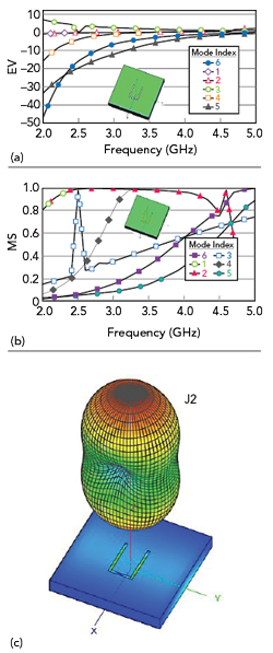
Figure 3 Slot antenna EV (a) and MS (b) vs. frequency; radiation pattern and surface current distribution (c).
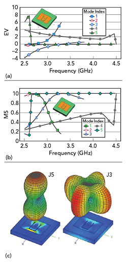
Figure 4 UMSA EV (a) and MS (b) vs. frequency; radiation patterns and surface current distributions (c).
U-Slot MSA (UMSA) Design
The UMSA is designed, combining MSA and U-slot designs, and the overall structure is shown in Figure 4. Figures 4a and b plot EV and MS versus frequency. Five modes are considered, i.e., J1 to J5 (mode indices varying from 1 to 5), and the figure shows that modes J3 and J5 contribute to the band of interest. Figure 4c plots the respective 3D radiation pattern and surface current distributions for modes J3 and J5 showing J5 provides the desired current distribution.
A probe excitation with a diameter of 1.35 mm is modeled to see its effect on CM propagation. Figure 5 plots the MECs versus frequency, confirming J5 as the desired radiation mode with a higher value of MEC near the resonant frequency. The inset in Figure 5 shows the surface current distribution, illustrating the in-phase coupling between the U-slot and the dominant TM10 mode of the MSA.14 The current distribution is maximum around the slot near the edges of the MSA.
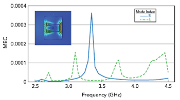
Figure 5 UMSA MEC vs. frequency.
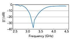
Figure 6 UMSA reflection coefficient magnitude vs. frequency.
Figure 6 plots the magnitude of the reflection coefficient, |Γ|, versus frequency using the standard Method of Moments (MoM) simulation. It shows that the desired bandwidth is achieved with resonance at 3.3 GHz. Note that the resonance point differs slightly from that determined with TCM.
The next section validates the design with two of the most promising and proven techniques available in prior literature40,41 to show TCM’s accuracy and effectiveness.
UMSA Design Validation
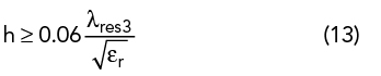
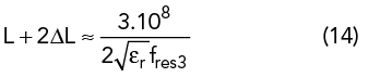
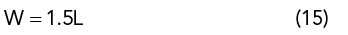
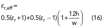
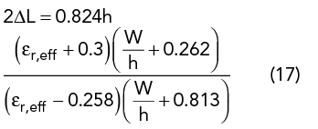
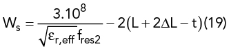
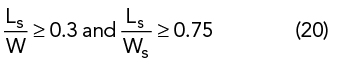
The initial UMSA design is obtained from closed-form empirical expressions using the dimensional invariance (DI)41 and three resonant frequency (TRF)40 techniques. TRF defines the criterion of choosing εr and h depending upon the desired FBW = 100 (fres2-fres4)/ fres3, where fres2 and fres4 are the lower and upper bounds of the VSWR bandwidth (2:1) and fres3 is the center frequency. The substrate thickness, h, must satisfy the criterion in Equation 13. Initial design parameters of the UMSA are chosen using Equation 13 to Equation 20 depending upon desired VSWR bandwidth40 (see Figure 1).
Ls is selected such that
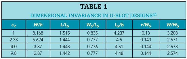
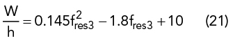
The DI method41 predicts that the only parameter dependent on substrate choice is W/h, and all other-dimensional parameters (see Figure 1) follow a constant ratio, as given in Table 1. A variation of W/h with frequency is studied and its empirical relationship is derived for the chosen substrate as
The UMSA is designed using TRF and DI techniques and compared with TCM. Table 2 summarizes the respective design variables with the achieved frequency band of operation. The three respective designs are simulated assuming the infinite substrate boundary conditions in MoM. Table 2 shows good agreement in terms of fres; however, the TCM agrees more closely with DI and yields a much more compact geometry compared to the one achieved using the TRF technique. This is because the DI technique also derives its respective ratios from MoM simulations41; therefore, both DI and TCM consider the fringe fields and finite edge effects. Thus, the design procedure using TCM is validated.

MC Analysis
MC behavior is described in 2 × 1 and 2 × 2 arrays. Figure 7 shows a 2 x 1 array as an inset and plots the self and mutual scattering parameters (SP) versus frequency. Over the 3 to 3.5 GHz band, the coupling |S21| is less than ‐18 dB and |Γ| = |S11| is less than ‐10 dB. Figure 8a shows a 2 × 2 array model and its respective SPs. |Γ| for all ports is less than ‐10 dB and MC is less than ‐18 dB over the 3 to 3.5 GHz band. A little variation in the resonance peaks of the four elements is observed due to the MC effect.17 Figure 8b shows the uniformly fed array radiation pattern. The HPBW is ∼54 degrees, Ge is ∼ 6.9 dBi and the peak sidelobe level is less than ‐13 dB.

Figure 7 UMSA self and mutual SPs.

Figure 8 UMSA 2 × 2 array self and mutual SPs (a) and radiation pattern (b).
Annular Ring Design
An annular ring (see Figure 9) is designed with dimensions based on the center frequency36 using (22):
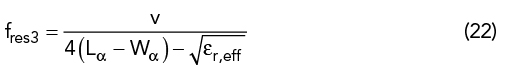
In (22), υ = 3×10⁸ m/s, Lα=LSIW‐(L+2c) = 42.21 mm and Wα = WSIW‐(W+2 d) = 39.21 mm. TCM identifies two resonances, 2.2 and 3.4 GHz for modes J1 and J4 (see Figures 9a and b), respectively. The dominant mode is the TM11 mode (J1) in this structure.

Figure 9 Annular ring EV (a) and MS (b) vs. frequency; surface current distribution and radiation pattern for modes J1 and J4 (c).

Figure 10 SIW CBMSA TCM EV (a), MS (b) and MEC (c) vs. frequency.
SIW Cavity-Backed UMSA (SIW CBMSA)
The annular ring with a PTH array adjoined to the UMSA (see Figure 1 and Figure 10) forms the SIW CBMSA structure. The dimensions are LSIW = 50.21, WSIW = 50.21, c = 4 and d = 5.5 mm. The PTH diameter is 1 mm, with a spacing of 2.875 mm, optimized to minimize leakage loss based on MC estimation between two adjacent antenna elements.
Figures 10a and b show EV and MS versus frequency considering four CMs, from Equation 12. An enhanced bandwidth is observed, contributed by modes J1, J2 and J3. Figure 10c plots MECs considering probe excitation and shows that J3 is the dominant mode while J1 contributes to a lesser degree.
Figure 11 shows the combined surface current distribution, J1+J3, and associated 3D radiation pattern at 3.3 GHz; normalized phi-cut distributions are also shown. An in-phase coupling between U-slot and patch edges is observed with minimal leakage to the annular ring, thus ensuring isolation from nearby structures. Ge is ∼6.9 dBi and HPBW is greater than 89 and 82 degrees in the respective planes.

Figure 11 SIW CBMPA radiation pattern and surface current distribution.
A bandwidth of 670 MHz (FBW = ∼20 percent) is shown by the dotted red curve in Figure 12. Figure 12 compares the simulated |Γ| obtained in an isolated environment with an infinite array environment generated using periodic boundary conditions (PBC).17,18 It also compares these with the measured |Γ| in an array environment. Generally good agreement is observed, with a slight difference between the PBC and measured results, due to neglecting the finite edges in the PBC environment.

Figure 12 Reflection coefficient magnitude vs. frequency.

Figure 13 SIW CBMA array (a) and mutual MC variation (b).
MEASURED RESULTS AND DISCUSSION
A 64 (8 × 8) SIW CBMSA array 500 × 500 mm2 in size is fabricated using standard photo-etching techniques. The inter-element spacing is 0.552λo along the x- and y-directions. It has a 5 mm-thick aluminum ground plane while ensuring that no air bubbles are formed in the structure (see Figure 13a).
The central element performance and the MC variation is measured (see Figure 13b). Coupling is measured between the central element and all other array elements. It is observed that the worst coupling is less than ‐20 dB, i.e., minimal leakage occurs from the SIW structure to its neighbors. Figure 12 shows the measured FBW is ∼22.5 percent (∼740 MHz), from 2.96 to 3.7 GHz for a VSWR less than 3:1, and 18 percent (∼600 MHz), from 3 to 3.6 GHz for a VSWR less than 2:1.

Table 3 summarizes the radiation parameters in the array environment measured in a planar near-field test measurement facility. The variation observed between the measured and the simulated parameters are attributed to the variation in h, due to the bonding of two layers of the substrate using a Rogers 3001 bonding film to achieve the desired thickness. The set targets are met from 3.1 to 3.5 GHz, showing Ge is greater than 8.4 dBi, the efficiency ηRE is greater than 95.2 percent (see Equation 23), cross-polarization is less than ‐22 dB and the HPBW is greater than 90 degrees in both principal planes except near the upper edge of the frequency band.
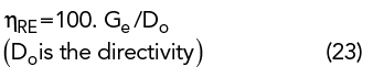

Table 4 compares SIW CBMSA performance with the prior work.33,42,27,25,43 Comparable performance with better efficiency, ηRE greater than 93.9 percent and FBW of ∼22 is shown. Figure 14 plots the measured co- and cross-polarized normalized radiation patterns in the array environment over the band, in the φ = 0- and 90-degree planes. A HPBW greater than 90 and 100 degrees in the two planes with cross-polarization less than ‐23 dB at boresight and better than ‐12 dB at extreme scan angles is demonstrated (see Table 3). The ripple level in the gain plots is less than ±0.5 dB.
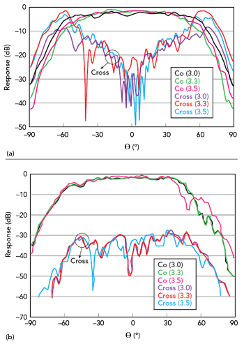
Figure 14 Measured co- and cross-polarization radiation patterns vs. θ at 3.0, 3.3 and 3.5 GHz with φ = 0 (a) and 90 (b) degrees.

Figure 15 Measured radiation pattern of the 64-element, uniformly fed array at center frequency.
Figure 15 shows the measured radiation pattern of a 64-element, uniformly fed array scanned to 0- and 45-degree angles. Ge decreases 1.15 dB from the peak value of ∼17.6 dBi at 0 degrees with no visible GLs, validating wide scan performance.
CONCLUSION
A simple design strategy based on TCM to design a broadband, broad beamwidth SIW CBMSA is presented. TCM provides insight into propagating CMs and shows that the choice of CM propagation in the constituent parts of the antenna helps achieve broadband performance. The resultant antenna design is validated in a 64-element array environment. The fabricated antenna’s measured performance agrees with the simulation and shows broad bandwidth and broad beamwidth. The results complement the existing literature and show promising applications to phased array antennas for various applications.
References
- R. J. Garbacz, A Generalized Expansion for Radiated and Scattered Fields, Ph.D. dissertation, Ohio State University, Columbus, 1968.
- R. Garbacz and R. Turpin, “A Generalized Expansion for Radiated and Scattered Fields,” IEEE Transactions on Antennas and Propagation, Vol. 19, No. 3, May 1971, pp. 348–358.
- R. F. Harrington and J. R. Mautz, “The Theory of Characteristic Modes for Conducting Bodies,” IEEE Transactions on Antennas and Propagation, Vol.19, No. 5, May 1971, pp. 622–628.
- R. F. Harrington, Field Computation by Moment Methods, Macmillan, New York, NY, 1968.
- Y. Chen and C.-F. Wang, Characteristic Modes: Theory and Applications in Antenna Engineering, Wiley, Hoboken, NJ, 2015.
- M. Vogel, G. Gampala, D. Ludick, U. Jakobus and C. J. Reddy, “Characteristic Mode Analysis: Putting Physics back into Simulation,” IEEE Antennas Propagation Magazine, Vol. 57, No. 2, April 2015, pp. 307–317.
- T.Y. Shih and N. Behdad, “Applications of the Characteristic Mode Theory to Antenna Design,” Developments in Antenna Analysis and Design (ed. Raj Mittra), Vol. 1, Scitech Publishing, U.K., 2018.
- X. Yang, Y. Liu and S. Gong, “Design of a Wideband Omnidirectional Antenna with Characteristic Mode Analysis,” IEEE Antennas and Wireless Propagation Letters, Vol. 17, No. 6, June 2018, pp. 993–997.
- C. Wang, Y. Chen and S. Yang, “Bandwidth Enhancement of a Dual-Polarized Slot Antenna Using Characteristic Modes,” IEEE Antennas and Wireless Propagation Letters, Vol. 17, No. 6, June 2018, pp. 988–992.
- Y. Luo, Z. N. Chen and K. Ma, “Enhanced Bandwidth and Directivity of a Dual-Mode Compressed High-Order Mode Stub-Loaded Dipole Using Characteristic Mode Analysis,” IEEE Transactions on Antennas and Propagation, Vol. 67, No. 3, March 2019, pp. 1922–1925.
- Y. Shi, Z. Meng, W. Wei, W. Zheng and L. Li, “Characteristic Mode Cancellation Method and its Application for Antenna RCS Reduction,” IEEE Antennas and Wireless Propagation Letters, Vol. 18, No. 9, September 2019, pp. 1784–1788.
- K. Kishore and S. Hum, “Multiport Multiband Chassis-Mode Antenna Design Using Characteristic Modes,” IEEE Antennas and Wireless Propagation Letters, Vol. 16, July 2016, pp. 609–612.
- J. Yang, J. Li and S. Zhou, “Study of Antenna Position on Vehicle by Using a Characteristic Modes Theory,” IEEE Antennas and Wireless Propagation Letters, Vol. 17, No. 7, July 2018, pp. 1132–1135.
- J. J. Borchardt and T. C. Lapointe, “U-Slot Patch Antenna Principle and Design Methodology Using Characteristic Mode Analysis and Coupled Mode Theory,” IEEE Access, Vol. 7, August 2019, pp. 109375–109385.
- Y. Chen and C. Wang, “Characteristic-Mode-Based Improvement of Circularly Polarized U-Slot and E-Shaped Patch Antennas,” IEEE Antennas and Wireless Propagation Letters, Vol. 11, November 2012, pp. 1474–1477.
- R. Garg, P. Bhartia, I. Bahl and A. Ittipiboon, Microstrip Antenna Design Handbook, Artech House, Norwood, Mass., 2001.
- N. Amitay, V. Galindo and C. P. Wu, Theory and Analysis of Phased Array Antennas, Wiley Interscience, Hoboken, N.J., 1972.
- C. Balanis (ed.), Modern Antenna Handbook, John Wiley & Sons, 2008.
- K. F. Lee, S. L. Steven Yang, A. A. Kishk and K. M. Luk, “The Versatile U-Slot Patch Antenna,” IEEE Antennas Propagation Magazine, Vol. 52, No. 1, February 2010, pp. 71–88.
- S. Bhardwaj and Y. Rahmat-Samii, “C-Shaped, E-Shaped and U-Slotted Patch Antennas: Size, Bandwidth and Cross-Polarization Characterizations,” 6th European Conference on Antennas and Propagation, March 2012, pp. 1674–1677.
- M. Khan and D. Chatterjee, “Characteristic Mode Analysis of a Class of Empirical Design Techniques for Probe-Fed U-Slot Microstrip Patch Antennas,” IEEE Transactions on Antennas and Propagation, Vol. 64, No. 7, July 2016, pp. 2758–2770.
- N. C. Karmakar, “Investigation into a Cavity-Backed Circular-Patch Antenna,” IEEE Transactions on Antennas and Propagation, Vol. 50, No. 12, December 2002, pp. 1706–1715.
- N. Vishwakarma, R. Samminga, A. Kedar and A. K. Singh, “Design Considerations for a Wide Scan Cavity Backed Patch Antenna for Active Phased Array Radar,” Indian Antenna Week, December 2011.
- K. Wu, “Integration and Interconnect Techniques of Planar and Non-Planar Structures for Microwave and Millimeter-Wave Circuits – Current Status and Future Trend,” Asia-Pacific Microwave Conference, December 2001.
- H. Liu, A. Qing, Z. Yu and S. Zhang, “Broad Band and Wide Scan SIW Cavity-Backed Phased Arrays for 5G Applications,” IEEE International Symposium on Antennas and Propagation, July 2019.
- Y. -Q. Wen, B. Wang and X. Ding, “Wide-Beam SIW-Slot Antenna for Wide-Angle Scanning Phased Array,” IEEE Antennas Wireless Propagation Letters, Vol. 15, January 2016, pp. 1638–1641.
- A. R. Vilenskiy, I. L. Vladimir and K. V. Lyulyukin, “Wideband Beam Steering Antenna Array of Printed Cavity-Backed Elements with Integrated EBG Structure,” IEEE Antennas Wireless Propagation Letters, Vol. 18, No. 2, February 2019, pp.245–249.
- Y. Cai, Y. Zhang, C. Ding and Z. Qian, “A Wideband Multilayer Substrate Integrated Waveguide Cavity-Backed Slot Antenna Array,” IEEE Transactions on Antennas and Propagation, Vol. 65, No. 7, July 2017, pp. 3465–3473.
- H. T Chou, T. W. Hsiao and J. H. Chou, “Active Phased Array of Cavity-Backed Slot Antennas with Modified Feeding Structure for the Applications of Direction-of-Arrival Estimation,” IEEE Transactions on Antennas and Propagation, Vol. 66, No. 5, May 2018, pp. 2667–2762.
- G. Q. Luo, T. Y. Wang and X. H. Zhang, “Review of Low-Profile Substrate Integrated Waveguide Cavity Backed Antennas,” International Journal of Antennas and Propagation, Vol. 2013, November 2013.
- A. Kumar and S. Raghavan, “A Review: Substrate Integrated Waveguide Antennas and Arrays,” Journal of Telecommunication, Electronic and Computer Engineering, Vol.8, No. 5, August 2016, pp.95–104.
- M. H. Awida, S. H. Suleiman and A. E. Fathy, “Substrate-Integrated Cavity-Backed Patch Arrays: A Low-Cost Approach for Bandwidth Enhancement,” IEEE Transactions on Antennas and Propagation, Vol. 59, No. 4, April 2011, pp. 1155–1163.
- M. H. Awida, A. H. Kamel and A. E. Fathy, “Analysis and Design of Wide-Scan Angle Wide-Band Phased Arrays of Substrate-Integrated Cavity-Backed Patches,” IEEE Transactions on Antennas and Propagation, Vol. 61, No. 6, June 2013, pp. 3034–3041.
- X. Zhang, S. Xiao, C. Liu, Z. Wang, J. Deng and X. Bai, “A Wideband and Circularly Polarized Wide-Angle Scanning Phased Array with Substrate-Integrated Cavity-Backed Patches,” International Conference on Microwave and Millimeter Wave Technology, May 2018.
- A. Kedar and A. Verma, “A SIW Based Microstrip Patch Antenna Array in X-Band for Phased Array Radar Applications,” IEEE Indian Conference on Antennas and Propagation, December 2019.
- S. Behera and K. J. Vinoy, “Microstrip Square Ring Antenna for Dual Band Operation,” Progress in Electromagnetics Research, Vol. 93, June 2009, pp. 41–56.
- A. Akdagli and A. Kayabasi, “An Accurate Computation Method Based on Artificial Neural Networks with Different Learning Algorithms for Resonant Frequency of Annular Ring Microstrip Antennas,” Journal of Computational Electronics, Vol. 13, No. 4, December 2014, pp. 1014–1019.
- Altair FEKO user manual, Suite 7.0, EM Software & Systems-S.A. (Pty) Ltd, 2014.
- H. G. Booker, “Slot Aerials and Their Relation to Complementary Wire Aerials (Babinet’s principle),” Journal Institution of Electrical Engineers - Part IIIA: Radiolocation, Vol. 93, No. 4, 1946, pp. 620–626.
- S. Weigand, G. H. Huff, K. H. Pan and J. T. Bernhard, “Analysis and Design of Broad-Band Single-Layer Rectangular U-Slot Microstrip Patch Antennas,” IEEE Transactions on Antennas and Propagation, Vol. 51, No. 3, March 2003, pp. 457–468.
- V. Natarajan and D. Chatterjee, “An Empirical Approach for Design of Wideband, Probe-Fed, U-Slot Microstrip Patch Antennas on Single-Layer, Infinite, Grounded Substrates,” Applied Computational Electromagnetics Society Journal, Vol. 18, No. 3, November 2003, pp. 191–200.
- P. Zhang, S. Qu and S. Yang, “Dual-Polarized Planar Phased Array Antenna with Cavity-Backed Elements,” IEEE Antennas and Wireless Propagation Letters, Vol. 18, No. 9, September 2019, pp. 1736–1740.
- J. Tan, W. Jiang, S. Gong, T. Cheng, J. Ren and K. Zhang, “Design of a Dual-Beam Cavity-Backed Patch Antenna for Future Fifth Generation Wireless Networks,” IET Microwaves Antennas & Propagation, Vol. 12, No. 10, May 2018.