
The Path to Lowest Phase Noise: A Fully Integrated Translation Loop
We are experiencing explosive growth in demand for bandwidth that pushes carrier frequencies to multiple decades of gigahertz. At these extremely high frequencies, consumers can enjoy wider bandwidth without fear of overcrowding the spectrum. However, as the frequencies increase, the instrumentation solutions targeting these devices and frequencies become extremely complex. This stems from the need for an order of magnitude better performance in instrumentation to prevent impairing the device under test. This article discusses several methods for low phase noise signal generation, describing the advantages and disadvantages of each and introducing the translation loop device, which takes the best of all frequency generation methods without their complexities to achieve ultra-low phase noise signal generation.

Figure 1 PLL block diagram.
Phase-locked loop (PLL) circuits are common in many frequency generation devices (see Figure 1). The PLL ensures the waveforms and signals created within a device are phase aligned or locked to a reference signal. The output of the voltage-controlled oscillator (VCO) is divided using an N counter and compared to a reference signal using the phase/frequency detector (PFD). The PLL is a simple circuit that has been extensively studied and the subject of numerous textbooks.1 We will use some of the well-known basics to establish what it takes to drastically reduce the phase noise at the output. Phase noise from each building block contribute to the overall phase noise of the PLL circuit. The phase noise associated with each block can be modeled, and the overall phase noise of the PLL precisely predicted, both through simulation and analytical calculation.
The PFD compares the reference signal to the divided output frequency. It produces an error signal that is fed to a charge pump circuit to create a control voltage, steering the VCO until the output phase of the device matches the reference phase. The data sheets for most frequency generation devices with integrated PFD circuits provide a figure of merit (FOM). Using the FOM, the in-band phase noise can be calculated as:
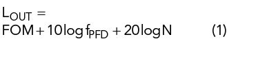
where fPFD is the PFD frequency and N the value of the output frequency divider. The output frequency is a multiplication of the fPFD and N divider value. For a given output frequency, as the fPFD increases by a factor, N decreases by the same factor. This results in lower overall output phase noise because any reduction in N reduces the phase noise by twice the rate of the increase from the fPFDterm. The greater the PFD frequency, the lower the close-in phase noise, which can be exploited to reduce the overall phase noise.
The loop filter follows the PFD and smooths the error signal from the PFD device that steers the VCO. It is designed using several parameters of the system: the charge pump current, VCO sensitivity and PFD frequency. One of the less emphasized functions of the loop filter is that it determines the bandwidth of the negative feedback control loop. The reference signal will influence the output signal’s phase noise within the control bandwidth of the loop filter. Beyond this cutoff frequency, the overall phase noise performance will be defined by the VCO characteristics. This fact will be used to optimize the overall phase noise of the system.
The VCO creates the output frequency based on the control voltage applied at its input. The VCO output frequency is updated by the control loop until it is phase-locked to the reference signal’s phase. The VCO directly influences the overall phase noise of the system. In general, as the quality factor of the VCO increases, its phase noise reduces.2 However, a higher quality factor usually requires components that limit VCO tunability. VCOs tuned for narrow frequency operation typically have the best phase noise performance.
FREQUENCY GENERATION
Instrumentation applications typically strive for the best performance, i.e., both low phase noise and spurious levels. Various oscillator topologies can be used to generate signals, which yield varying levels of quality. These include:
Fixed Frequency Oscillators

Figure 2 Variable frequency generation using a fixed source.
Fixed frequency oscillators are signal generation devices that have excellent phase noise performance. These devices typically have very high-quality factors, enabling superior close-in phase noise performance. They operate at a predetermined frequency, largely defined by the geometry and the construction of the device, with some tunability to enable phase-locking to a reference source. Oven controlled crystal oscillators (OCXOs), temperature compensated crystal oscillators (TCXOs) and voltage-controlled surface acoustic wave (SAW) oscillators are some examples of these devices. One key disadvantage of fixed frequency oscillators is their limited frequency coverage. While they may be suitable for devices operating at a fixed set of frequencies or multiples of those frequencies, most instrumentation devices require variable frequency coverage.

Figure 3 Output spectrum (a) and phase noise (b) of the AD9164 at 800 MHz, using a fixed frequency oscillator as the sampling clock.
Using a direct digital synthesis (DDS) or digital-to-analog converter (DAC) is one solution to this problem (see Figure 2). The fixed frequency signal can be used to drive the sampling clock of a DDS device, with the oscillator’s frequency multiplied as needed through a frequency multiplier or a step recovery diode and filtered before it is applied to the DDS. The DDS can create any arbitrary frequency up to half the sampling frequency in the first Nyquist zone of operation. Some modern DACs can even operate comfortably in the second Nyquist zone.
Figure 3 shows an example of the output spectrum and phase noise of the Analog Devices AD9164 driven by a low phase noise dielectric resonator oscillator at 6 GHz. The phase noise plot shows incredibly low output phase noise, with output spectrum spurs less than -70 dBc.
The spectral purity of the multiplied sampling clock has a direct influence at the output of the device. Once the signal is multiplied, many harmonics will be present at the output. Typically, the spurs at the sampling clock will appear at the output at similar levels. The desired signal then needs to be filtered to achieve very low spurious levels at the output of the DDS. For large multiplication factors, the filters may need to be extremely sharp, which can require significant area.
The phase noise of the multiplied signal increases as the multiplication factor increases. For example, every time the signal frequency is doubled, the phase noise increases by 6 dB. Based on the starting phase noise profile and multiplication factor, the noise floor of the far-out phase noise can increase significantly, making the overall solution less appealing. This is a well-known dilemma, where leveraging the close-in phase noise of a single frequency, high-quality factor device comes with a far-out phase noise floor penalty. As an example, SAW devices have excellent close-in phase noise performance, with carrier frequencies around 1 GHz. Using one for a mmWave application operating above 40 GHz would require multiplication as high as 40, which could result in greater than a 32 dB increase in the phase noise floor, which could make the solution less appealing.
Wideband PLL Devices
Wideband synthesizers solve many of the challenges associated with single frequency devices. These use multiple VCO cores that are further divided into multiple overlapping bands. This architecture enables each core and band to be designed with a high-quality factor. This significantly improves the overall performance of the device compared to architectures using a single core. One key advantage of these devices is higher fundamental operating frequencies compared to crystal or SAW-based oscillators. Many modern VCOs can have fundamental frequencies from 4 to 20 GHz or higher. This makes their far-out phase noise in mmWave applications much more appealing. For example, a device operating at a 10 GHz fundamental frequency only requires multiplication by 4x to extend the frequency to 40 GHz, which translates to a phase noise floor increase of 12 dB, compared to a 32 dB increase using a crystal oscillator.
One challenge associated with multicore and multiband devices is finding the optimum band to synthesize the target frequency. This could involve creating lookup tables to identify the correct band. Devices equipped with autocalibration features make this process much easier and robust to temperature and process variations. This vastly simplifies the overall operation of the device, where frequency changes can simply be programmed into the registers of the device and the optimum band automatically determined. Another challenge with this option is that the close-in phase noise of these devices is typically much higher compared to single frequency devices. Even with the lower overall phase noise floor, the higher close-in phase noise can result in higher overall integrated noise, limiting their use in applications that demand lower integrated phase noise.
Translation Loop

Figure 4 Translation loop architecture.
The translation loop takes the best of all these frequency generation methods without their disadvantages. To see why, recall that single frequency devices such as OCXOs, SAWs and crystals with high-quality factors have the best close-in phase noise. These single frequency devices usually have low fundamental frequencies, making the far-out phase noise less appealing when they are multiplied to mmWave frequencies. An ideal solution would take advantage of the close-in performance of these devices without the far-out phase noise penalty. DDS or DAC devices can be used to generate variable frequencies using fixed frequency devices. These also suffer from the large multiplication factors needed for mmWave frequencies and filtering to reject subharmonics and other spurs. Tolerating these shortcomings can enable a desirable solution. Wideband synthesizers can have very high fundamental frequencies with excellent far-out phase noise performance. However, these devices do not really have high-quality factors, making the close-in phase noise relatively poor compared to single frequency devices. Leveraging the far-out phase noise without the degraded close-in phase noise would be necessary.

Figure 5 Phase noise profile of a translation loop device.

Figure 6 Translation loop output spectrum at 6.5 GHz (a) and LO input spectrum at 3 GHz (b).
This brings us to the translation loop device (see Figure 4). Instead of dividing the output frequency by a large divider value, a frequency mixer is used to shift the output signal to an intermediate frequency (IF) that matches the reference signal’s frequency. This effectively reduces the divider value to 1, eliminating the noise contribution originating from the typically large divider values used in traditional PLL devices. This also imposes the phase noise profile of the local oscillator (LO) on the control loop. A single frequency device with excellent close-in performance and a DDS can be used to create this LO signal.
The loop filter bandwidth is a critical design parameter for the translation loop device. As discussed, the loop filter determines the overall bandwidth of the control loop, i.e., it defines how far the reference and LO signal influence the output phase noise. We can choose a large loop filter bandwidth for the translation loop since the close-in phase noise can be extremely low. Figure 5 shows the phase noise profile of a translation loop device and its LO input. The figure shows the LO phase noise, which is extremely low close-in but has a high far-out noise floor. However, the phase noise of the RF output only tracks the LO phase noise up to the loop filter bandwidth. After this frequency offset, the far-out phase noise is defined by the VCO, which is extremely low. By selecting a large loop bandwidth, the translation loop device leverages the desirable close-in performance of a single frequency device using a DDS as an LO and the far-out phase noise of a wideband VCO. This approach breaks the well-known dilemma about which phase noise region to optimize, resulting in extremely low output phase noise.
The superior phase noise performance of the translation loop makes it very useful in many mmWave instrumentation applications. In addition to low phase noise performance, instrumentation is also expected to suppress spurious signals to extremely low levels. This can be tremendously challenging with translation loop devices because of several strong signals at different frequencies. In many cases, it is challenging to prevent feedthrough of the LO and intermediate frequency (IF) signals to the output. Further, many intermodulation products of the IF, LO and RF can be created at the output, and these spurious signals can cause the overall instrumentation solution to have poor spurious performance.
An example of a translation loop device which addresses these challenges, the Analog Devices ADF4401A eliminates all the feedthrough paths that could exist in a discrete implementation with built-in shielding and design practices minimizing feedthrough. The result is spur rejection of -90 dBc, which rivals yttrium iron garnet sphere-based oscillators.
The output of the ADF4401A can have low spur levels even if the inputs to the system are less than ideal. Figure 6a shows the output spectrum with an LO input that contains many spurs around -40 dBc (see Figure 6b). Typically, this type of an LO signal is not usable in instrumentation because of the extensive amount of filtering needed. However, the ADF4401A can accept this LO input without requiring additional filtering, producing the output shown in Figure 6a. The device has an autocalibration engine to identify the optimum VCO band for a given target frequency. In the calibration mode, the device searches for the correct band under actual temperature and process conditions, making frequency tuning streamless.
SUMMARY
Instrumentation solutions require very low phase noise carrier signals with extremely low spurious levels to meet the demands of mmWave systems. While various methods are used to synthesize these signals, all have significant trade-offs, making a solution complex. The translation loop architecture leverages the advantages of several frequency generation options - without the disadvantages - to achieve ultra-low phase noise and spurious signals without complex filtering.
References
- I. Collins, “Phase-Locked Loop (PLL) Fundamentals,” Analog Dialogue, Vol. 52, No. 3, July 2018.
- D. B. Leeson, “A Simple Model of Feedback Oscillator Noise Spectrum,” Proceedings of the IEEE, Vol. 54, No. 2, February 1966.