
Broadband, High Efficiency, Class J Power Amplifier Design Method with Compensating Drain-Source Capacitance
A broadband, high efficiency, class J power amplifier (PA) design uses the relationship between drain efficiency and the ratio of drain-source capacitance to load impedance. In addition, multi-section matching is applied at the input and output to expand the bandwidth. A wideband class J PA designed with this approach and a Wolfspeed CGH40010F GaN HEMT achieved 40.0 to 41.5 dBm output power with 60 to 68 percent drain efficiency and an adjacent channel power ratio better than -30 dBc from 1.4 to 3.6 GHz.
With the rapid development of modern wireless communication technology, the amount of information transmitted is increasing and requiring wider bandwidth. This inevitably challenges the design of broadband PAs for wireless transmitters. The class J PA proposed by S.C. Cripps in 20061 uses drain-source capacitance, Cds, to control harmonics at the output of a conventional class AB power amplifier to achieve high efficiency.2 In recent years, several methods for expanding the bandwidth of class J amplifiers have been reported.3-6 Saxena et al.3 designed a continuous class J PA using the nonlinear embedding approach, achieving between 63 and 72 percent drain efficiency from 1.3 to 2.4 GHz. Friesicke et al.4 proposed a resistive-reactive class J PA with complex load impedances to explore efficiency-bandwidth tradeoffs in wideband class J designs with lossy second-harmonic loads. Andersson et al.5 described a class J PA with dynamic load modulation to obtain output power and high efficiency over a certain dynamic range, and a broadband, high efficiency PA based on hybrid continuous modes with a phase shift parameter was reported by Huang et al.6
In this article, a design method based on traditional class J PA theory, which predicts high efficiency within a certain range of Cds/RL, is described. This work analyzes the trend of drain-source capacitance with the drain-source voltage and proposes a circuit to compensate transistor output capacitance so that Cds/RL can remain in the high efficiency range. A wideband J PA was designed and fabricated to validate the approach.
ANALYSIS AND DESIGN
Based on traditional theory, the transistor output voltage for an ideal class J PA can be expressed as4
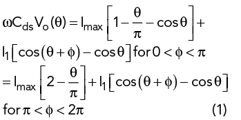
where Imax is the maximum output current of the drain, I1 is the output fundamental current, φ is the conduction angle, Cds is the transistor drain-source capacitance and θ is a simple representation of the matching circuit phase, its value is determined by the parameters of each part of the output matching circuit.
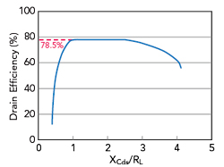
Figure 1 Drain efficiency vs. XCds/RL.
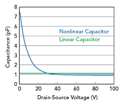
Figure 2 Output capacitance variation vs. drain-source voltage.
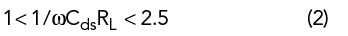
The relationship between drain efficiency and XCds/RL is shown in Figure 1 under ideal conditions,1 showing the drain efficiency remains at the ideal 78.5 percent when the value of XCds/RL is between 1 and 2.5:
This range provides additional space for the design of a broadband, high efficiency, class J PA.
Considering an ideal class B amplifier, RL can be expressed as
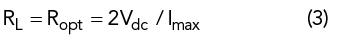
where Ropt is the optimal load impedance and Vdc is the drain DC bias voltage. The transistor output capacitance in pF is
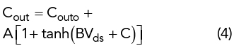
where Cout is the output capacitance of transistor and Couto, A, B and C are constants associated with the transistor. For the Wolfspeed CGH40010F GaN HEMT, Couto = 0.95, A = 1192.4, B = -0.0594714 and C = -2.94696.7
According to Equation 4, the relationship between the output capacitance and the drain voltage is shown in Figure 2. When the drain-source voltage Vds is small, i.e., less than approximately 28 V, the transistor output capacitance decreases nonlinearly as the drain-source voltage increases. Beyond Vds = 28 V, the capacitance reaches a constant value of 1.185 pF.
As the input signal power level has a direct impact on the magnitude of the drain signal power, changes in transistor output capacitance are discussed separately for low and high input power levels. For low input power, the effect of drain AC signal power can be ignored compared to the DC bias. The output capacitance is approximately 1.185 pF for a DC bias of Vds = 28 V. If the maximum current Imax is about 1.5 A, the theoretical high efficiency frequency range of operation is 1.44 to 3.61 GHz, found by applying Equations 2 and 3, and the corresponding drain efficiency is 78.5 percent. For large input power, the drain AC signal power has an obvious impact on the DC drain bias. For Vds = 28 V, the output capacitance is nonlinear. The relationship between the capacitive reactance, XCds, and drain-source voltage is plotted in Figure 3, showing the capacitive reactance increases as frequency decreases and drain-source voltage increases.
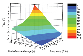
Figure 3 Output capacitive reactance variation vs. drain-source voltage and frequency.
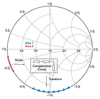
Figure 4 Impedance transformation of XCds to compensate for the nonlinear change in capacitance.
An external compensation circuit is needed to compensate for the nonlinear changes in capacitance so XCds/RL can remain in the high efficiency region. The capacitive reactance, XCds, varies from -5.88 to -93.27 Ω. Area 1 in Figure 4 shows that the impedance of the minimum capacitance value (1.18 pF) from 1.44 to 3.61 GHz varies from -93.27 to -37.20 Ω, which is ideal for high drain efficiency. Area 2 indicates that the impedance of the maximum capacitance value (9 pF) over the same frequency range varies from -14.73 to -5.88 Ω. In this work, the impedances of area 2 are transformed to those of area 1 (XCds/RL = 1 to 2.5) by designing an appropriate output compensation circuit. The circuit in Figure 4 is a simple two-stage microstrip series section and shunt open stub. By selecting the appropriate microstrip parameters, this simple structure provides the desired compensation when connected at the output.
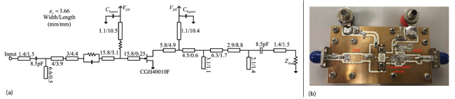
Figure 5 Class J PA schematic (a) and assembled amplifier (b).
MEASUREMENT RESULTS
To validate the design method, a broadband, high efficiency, class J PA was fabricated using the Wolfspeed CGH40010F GaN HEMT transistor and a Rogers 4350B substrate. The device was biased at Vds= 28 V and Vgs = -2.8 V. To achieve broadband performance, the bias network was considered when performing input-output matching, which reduces the power leakage over a wide frequency band and improves output power and efficiency. The transistor packaging model was embedded in the output matching circuit to reduce the influence of parasitics. In addition, a multi-step matching method was used to increase bandwidth.
A schematic and a photograph of the class J PA are shown in Figure 5. Figure 6 compares measurements with simulation for gain, output power and drain efficiency over the 1.4 to 3.6 GHz frequency band. Output power at 2 dB compression was 39.7 to 41.2 dBm, with drain efficiency of 60 to 68 percent and gain from 9.8 to 13.2 dB. Figure 7 shows the ACPRs using a 5 MHz WCDMA signal, demonstrating -27.1 to -37.5 dBc over the band.
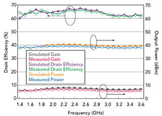
Figure 6 Measured vs. simulated drain efficiency, saturated output power and gain.
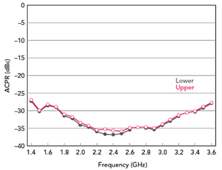
Figure 7 Measured ACPR.
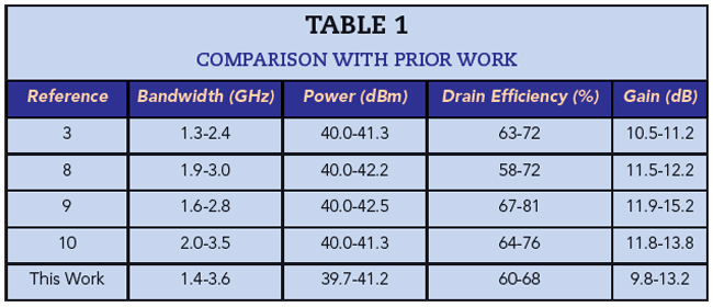
Table 1 compares these results with the performance of other published broadband PAs. Although similar in most other respects, this design approach achieves greater bandwidth: approximately 88 percent compared to the 45 to 59 percent range reported for the other designs.
CONCLUSION
An optimum output capacitor impedance space for a wideband, high efficiency, class J PA was defined and corresponding compensation circuit designed. A stepped impedance circuit was also adopted for input and output matching, accounting for transistor package parasitics to extend the bandwidth.
Acknowledgment
This work was supported by the Zhejiang Provincial Natural Science Foundation (Grant LZ16F010001) and National Natural Science Foundation (Grant 61871169).
References
- S. C. Cripps, RF Power Amplifiers for Wireless Communications, Artech House Publishers, Second Edition, 2006.
- P. Wright, J. Lees, P. J. Tasker, J. Benedikt and S. C. Cripps, “An Efficient, Linear, Broadband Class J Mode PA Realised Using RF Waveform Engineering,” IEEE MTT-S International Microwave Symposium Digest, June 2009, pp. 653–656
- S. Saxena, K. Rawat and P. Roblin, “Continuous Class-B/J Power Amplifier Using Nonlinear Embedding Technique,” IEEE Transactions on Circuits and Systems - II: Express Briefs, Vol. 64, No. 7, July 2017, pp. 837–841.
- C. Friesicke, R. Quay and Arne F. Jacob, “The Resistive-Reactive Class-J Power Amplifier Mode,” IEEE Microwave and Wireless Components Letters, Vol. 25, No. 10, October 2015, pp. 666–668.
- C. M. Andersson, D. Gustafsson, K. Yamanaka, E. Kuwata, H. Otsuka, M. Nakayama, Y. Hirano, I. Angelov, C. Fager and N. Rorsman, “Theory and Design of Class-J Power Amplifiers With Dynamic Load Modulation,” IEEE Transactions on Microwave Theory and Techniques, Vol. 60, No. 12, December 2012, pp. 3778–3786.
- C. Huang, S. He, W. Shi and B. Song, “Design of Broadband High-Efficiency Power Amplifiers Based on the Hybrid Continuous Modes With Phase Shift Parameter,” IEEE Microwave and Wireless Components Letters, Vol. 28, No. 2, February 2018, pp. 159–161.
- J. Moon, J. Kim and B. Kim, “Investigation of a Class-J Power Amplifier with a Nonlinear Cout for Optimized Operation,” IEEE Transactions on Microwave Theory and Techniques, Vol. 58, No. 11, November 2010, pp. 2800–2811.
- X. Meng, C. Yu, Y. Liu and Y. Wu, “Design Approach for Implementation of Class-J Broadband Power Amplifiers Using Synthesized Band-Pass and Low-Pass Matching Topology,” IEEE Transactions on Microwave Theory and Techniques, Vol. 65, No. 12, December 2017, pp. 4984–4996.
- J. Chen, S. He, F. You, R. Tong and R. Peng, “Design of Broadband High-Efficiency Power Amplifiers Based on a Series of Continuous Modes,” IEEE Microwave and Wireless Components Letters, Vol. 24, No. 9, September 2014, pp. 631–633.
- J. Xia, X. W. Zhu and L. Zhang, “A Linearized 2–3.5 GHz Highly Efficient Harmonic-Tuned Power Amplifier Exploiting Stepped-Impedance Filtering Matching Network,” IEEE Microwave and Wireless Components Letters, Vol. 24, No. 9, September 2014, pp. 602–604.