
Characterization of Additive Phase Noise in Microwave Amplifiers
High-power signals with minimal phase noise are crucial for radar and communication systems, for phase noise is directly related to receiver sensitivity. At the heart of each system is an oscillator, which can be configured to have very low phase noise. However, oscillators tend to have low output power, so they often must be boosted by amplifiers. The addition of amplifiers presents other issues, most notably the addition of phase noise to signals passing through the system. This additive phase noise can mask a target or otherwise interfere with signal integrity and transmission.

Figure 1 Phase noise contributors in oscillators.

Figure 2 An amplifier's effect on phase noise.

Figure 3 Phase noise measurement setup.
One serious issue faced by systems designers is quantifying the level of additive phase noise, since this parameter is challenging to measure. In this article, we discuss additive phase noise and the reasons why reducing an amplifier’s contribution to phase noise is important to a system’s performance. We also demonstrate the techniques needed to improve additive phase noise measurements across frequencies for reliable product classification. We further investigate the impact of amplifier type and compression level on additive phase noise and explore how the optimization of these characteristics can improve phase noise performance dramatically. Finally, we verify our findings through production testing and convey the ramifications for engineering design.
ADDITIVE PHASE NOISE
Phase noise refers to the stability of a signal’s frequency over time.1–3 Ideally, an oscillator produces a perfect sinusoid at a singular frequency -- which we call the carrier or desired signal -- that has zero phase noise. However, the presence of noise causes all oscillators to behave in a non-ideal fashion. The two main sources of phase noise are background noise and the up-conversion of near DC (1/f) flicker noise (see Figure 1).
As the figure shows, background noise is constant over time and dominates the high frequency spectrum away from the source frequency. The power of the background noise, PN, is defined as
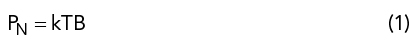
where k is Boltzmann’s constant, B the frequency bandwidth and T the temperature of the system. The background noise is, therefore, related to operating conditions in addition to the oscillator itself.
The other type of phase noise, the up-conversion of flicker noise, manifests as a skirt around the desired frequency, rather than a single tone in the frequency domain. As shown in Figure 1, flicker noise decreases linearly on the logarithmic scale until it reaches the corner frequency, which is where the spectrum becomes dominated by the high frequency background noise. Since this second source of phase noise is produced close to the carrier, it causes significant signal interference.
In a system requiring high sensitivity, an oscillator with low absolute phase noise is an ideal signal generator. However, many applications require higher power levels than a standard signal generator can produce, so amplification must be introduced into the transmit chain. Rather than solely amplifying the oscillator’s carrier signal and associated phase noise skirt, though, the amplifier adds phase noise of its own (see Figure 2). As shown in this figure, the width and height of the output skirt increases due to the additive phase noise of the amplifier. If an amplifier’s phase noise is too high, it can overpower the noise associated with the oscillator, eliminating the benefits of a low noise oscillator. As a result, properly characterizing and measuring the phase noise of amplifiers and other components is important to ensure the successful performance of RF systems.
ADDITIVE PHASE NOISE MEASUREMENT
Additive phase noise can be notoriously difficult to measure because it is often 30 to 40 dB lower than the absolute phase noise of the reference signal.3,4 Therefore, phase cancellation is used to perform the measurement. This method has been examined by Breitbarth and Koebel5 and implemented in commercially available phase noise analyzers, such as the Holzworth Instrumentation HA7701A used in this study. A block diagram of the measurement setup is shown in Figure 3, including the internal components of the analyzer. The block diagram shows how the phase cancellation measurement system isolates the amplifier additive phase noise.
The reference signal provides the source power for the system and is split to power the local oscillator (LO) and RF paths separately. The RF path passes through the device under test and includes attenuators to set the appropriate drive level. The attenuators before the amplifier control input power and compression level, since high power can overdrive the amplifier. The attenuators after the amplifier protect the internal mixer; they impact the phase noise readings by approximately 1 dB, depending on the amount of attenuation. If the output power from the amplifier is very low, minimizing the RF drive attenuation is beneficial to ensure the phase noise analyzer can detect the input signal.
The LO path includes a variable delay line and a 90-degree phase shifter to maintain quadrature between the LO and RF paths. Phase cancellation is highly dependent on LO and RF phase matching, so the variable delay is important to overcome inherent errors in the phase shifter. By performing manual adjustments to the LO path, we have seen measurements improve up to 4 dB. Short cables and low loss paths are needed on the LO side to ensure sufficient input power to the mixer, helping compensate for the output power limitations of standard signal sources, especially at higher frequencies. High LO drive of 15 to 18 dBm reduces the amplitude modulation (AM) noise in the phase detector, which lowers the system measurement floor. After the mixer cancels out the reference signal, the signal that remains represents the additive phase noise associated with the amplifier. The phase noise analyzer amplifies this using an internal low noise amplifier (LNA) and the voltage signal is applied to an analog-to-digital converter. The resulting trace provides a sweep of the single sideband phase noise by offset frequency.
Using this measurement technique, we measured amplifiers from Qorvo’s standard products line, testing different power levels and frequencies. Table 1 summarizes the median phase noise for four amplifiers. Compared to the reference signal’s phase noise of about -120 dBc/Hz, the low phase noise values measured show the effectiveness of the test system’s noise cancellation.

AMPLIFIER TRENDS
As shown in the table, the phase noise of the four amplifiers - low noise, driver and wideband distributed amplifiers - varies from approximately -150 to -165 dBc/Hz. To explain the differences, we compared amplifier topologies, but found it is not a defining factor. Rather, the differences are largely determined by device technology.

Figure 4 HBT (CMD274) vs. PHEMT (CMD316) amplifier phase noise, both in saturation at 6 GHz.
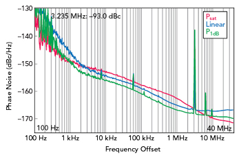
Figure 5 CMD315 PHEMT amplifier phase noise vs. signal level at 6 GHz.
Figure 4 compares the phase noise of a PHEMT amplifier (CMD316) to one using HBTs (CMD274). The phase noise measurement of the HBT amplifier is 10 to 15 dB lower than the PHEMT amplifier when operated in saturation and at the same frequency. Although PHEMT amplifiers have higher output power and frequency capabilities than HBT amplifiers, they typically have worse phase noise. Compared to PHEMTs, HBTs have lower electron mobility, leading to less fluctuations in charge and electron movement within the device channels.6 Less variation contributes to fewer up-conversions in HBT amplifiers, so they have considerably lower phase noise than PHEMT amplifiers.7
A second trend investigated for PHEMT and HBT amplifiers was the relationship between phase noise and amplifier compression, concentrating on the three main regions of an amplifier’s transfer characteristic: linear, saturated and 1 dB compression. In an amplifier’s linear region, the output power is directly proportional to input power. At saturation (Psat), an amplifier produces no additional output power as input power increases. At 1 dB compression (P1dB), the gain of the amplifier is reduced by 1 dB from its linear level, an intermediate region between linear and saturated operation. To compare the phase noise of these three states, we used attenuation to regulate the amplifier’s input power to consistently measure performance and see the trends.
Figure 5 shows phase noise measurements of a PHEMT amplifier (CMD315) driven at different levels of compression. The phase noise is a minimum at P1dB, achieving -156.3 dBc/Hz at 10 kHz offset, a significant phase noise improvement versus being operated at either linear or Psat. At frequencies close to the carrier, many other amplifiers show the same trend in phase noise versus compression, i.e., the phase noise is typically minimized at P1dB, followed closely by the linear drive region. Saturated operation generally leads to the highest phase noise, often 3 to 4 dB higher when compared to P1dB.
We believe the optimal result at P1dB can be explained considering the distortion in amplifiers caused by amplitude-to-amplitude (AM-AM) and amplitude-to-phase (AM-PM) modulation. AM-AM refers to the change in an amplifier’s output amplitude depending on the input power level, while AM-PM refers to the change in the output phase of a signal depending on changes in the input amplitude. Each type of modulation contributes to the additive phase noise of an amplifier, so minimizing these distortions will minimize the overall noise.
The AM-AM and AM-PM distortions on the CMD315 PHEMT amplifier are shown in Figure 6. Note that the AM-AM and AM-PM trends appear to correlate closely to amplifier saturation levels. One explanation may be the following: In the linear region (less than 0 dBm input power), both the AM-AM and AM-PM distortions are minimized. Any AM noise at the input will appear primarily as amplified, undistorted AM noise at the output and will cause minimal additional phase noise. As the amplifier enters compression around 2 dBm input power, its gain roll-off attenuates the AM-AM noise and lessens its impact on phase deviation at the output. At the same time, however, the AM-PM phase distortion begins to grow. The AM-PM distortion increases as the amplifier reaches deep saturation, while the impact from the AM-AM noise is lessened further. Therefore, it appears the contribution to an amplifier’s additive phase noise is maximized in the linear region by AM-AM noise and maximized in the saturated region by AM-PM distortion. However, as shown in Figure 5, the lowest phase noise of the CMD315 amplifier is at P1dB. This region represents a near ideal situation where the AM-AM distortion is partially suppressed, while the AM-PM distortion is still small, less than 2 degrees at 2 dBm of input power (see Figure 6). Operating the amplifier at P1dB yields the minimum overall noise of the device and, therefore, the lowest additive phase noise. Many GaAs PHEMT and HBT amplifiers follow this trend; however, it may not be universal across all amplifiers, especially where the AM-PM distortion is greater at lower input power.

Figure 6 AM-AM and AM-PM distortion of the CMD315 PHEMT amplifier at 6 GHz.
Finally, note a curious phenomenon in Figure 5, where the trends in phase noise change for frequency offsets of 2 MHz or greater. At these higher offset frequencies, Psat becomes the preferred cooperating level to achieve the lowest phase noise.8 This relationship is governed by

where L is the phase noise after the spectrum levels out, -177 is the power of the thermal noise floor at room temperature, Pin is the input power to the amplifier and NF is the amplifier’s noise figure. As an amplifier enters saturation, its input power increases at a much faster rate than its output noise, resulting in decreasing phase noise at high offset frequencies. As we were more concerned about the impact of phase noise at lower offsets, e.g., <100 kHz, we did not investigate this trend further.
PHASE NOISE VARIABILITY
As phase noise will certainly vary from part-to-part and between lots, it is important for system engineers to know the bounds of this variation. We tested phase noise on production lots of the CMD264, a standard product LNA, to confirm the relationships between phase noise and power were consistent for all units in a lot. The packaged parts were manually tested using an expanded phase noise analysis setup, which included a manual production test fixture and longer cables. Since the apparatus reduced connectivity and drive power levels, the average phase noise measured across the lot increased slightly compared to the initial baseline.

Figure 7 CMD264 phase noise distribution at 10 kHz offset from an 8 GHz carrier at 1 dB compression.
Figure 7 shows the phase noise distribution at 10 kHz offset for 78 units within a single lot at P1dB. The phase noise variation fits a normal distribution about the mean for all units tested. Phase noise values have a range of about 1.3 dB and a standard deviation of 0.3 dB, a relatively tight distribution for the part. The similarities indicate that phase noise is related more to the semiconductor process used for an amplifier, rather than manufacturing deviations among the units. Also, this margin of error is small enough that the relationship between compression and phase noise cannot be discounted as a measurement error.
CONCLUSION
In this article, we examined the use of a phase cancellation technique for making accurate additive phase noise measurements. We also identified methods for improving the system noise floor performance and optimizing the phase detector to enhance measurement capabilities. Using these techniques, we explored phase noise trends considering the amplifier’s semiconductor process and compression level. We also validated these trends by testing amplifiers in a single lot to demonstrate phase noise consistency.
To minimize additive phase noise, we recommend selecting an HBT amplifier. To optimize the phase noise of PHEMT amplifiers, we recommend operating at P1dB to minimize both AM-AM and AM-PM distortion. If operation at P1dB is not feasible, then the linear region provides the next lowest phase noise. Overall, we strongly recommend considering phase noise capabilities when choosing an amplifier for sensitive RF systems.
Acknowledgments
The authors acknowledge the following colleagues for their contributions to this work: Joe Koebel and Aaron Potosky of Holzworth Instrumentation, for information about the functionality of the phase noise analyzer; R&S, for allowing access to the FSWP phase noise analyzer and the SMA signal generator to validate our findings; Keysight, for confirming our measurements during a virtual demo; Bob Festa, Paul Jackson and Pete Rutigliano of Qorvo, for their technical assistance in the lab and Helen Leung, for creating the block diagram of the phase noise measurement setup.
References
- Custom MMIC, “Addressing Phase Noise Challenges in Radar and Communication Systems.”
- E. Rubiola and R. Boudot, “Phase Noise in RF and Microwave Amplifiers,” 2010 IEEE International Frequency Control Symposium, 2010, pp. 109–111.
- “Mastering Phase Noise Measurements” Rohde & Schwarz, Oct. 2016.
- D. Owen, “Good Practice Guide to Phase Noise Measurement,” National Physical Laboratory, May 2004.
- J. Breitbarth and J. Koebel, “Additive (Residual) Phase Noise Measurement of Amplifiers, Frequency Dividers and Frequency Multipliers,” Microwave Journal, Vol. 51, No. 6, June 2008, pp. 66–72.
- A. Dasgupta, S. Khandelwal and Y. S. Chauhan, “Compact Modeling of Flicker Noise in HEMTs,” IEEE Journal of the Electron Devices Society, Vol. 2, No. 6, Nov. 2014, pp. 174–178.
- P. J. Garner, M. J. Howes and C. M. Snowden, “Ka-band and MMIC pHEMT-based VCO’s with Low Phase-noise Properties,” IEEE Transactions on Microwave Theory and Techniques, Vol. 46, No. 10, Oct. 1998, pp. 1531–1536.
- N. Garmendia and J. Portilla, “Study of PM Noise and Noise Figure in Low Noise Amplifiers Working under Small and Large Signal Conditions,” 2007 IEEE/MTT-S International Microwave Symposium, 2007, pp. 2095–2098.