
Online Spotlight: Primer on the Use of Digital Control and a Delay Line to Frequency Lock an Oscillator
Countless applications require stable high frequency signal sources. Unfortunately, oscillator noise inherently increases with frequency. A frequency lock loop is a solution which has been around for many years; design techniques and analysis are well understood. The typical tradeoff is between a high frequency source that is unstable vs. a low frequency source that is very stable; and, by locking the two signal sources together, the best of both worlds can be achieved. An alternative is the use of a delay line; the circuit uses the one high frequency source, delayed in time, as its own frequency reference, eliminating the need for a second stable low frequency source. Most designs employ exclusively analog elements. An uncommon variation replaces certain analog elements with digital elements. This article outlines the design of a stable high frequency signal source utilizing a delay line approach with both analog and digital components. It also includes a brief discussion on the software required to control and linearize the circuit.
There are many approaches to frequency lock oscillator design. The circuit in Figure 1 captures the basic elements. A voltage-controlled oscillator (VCO) is driven by a control voltage, Vc. The output of the VCO is routed to an element that can “sense” a frequency variation, or drift. An element must also be included that can “compensate” for that drift. The output of the “compensate” element (the error voltage) is summed with a control voltage and fed back to the VCO in order to oppose unwanted frequency drift. The circuit in Figure 1 is a generic solution. Although there are many architectures to accomplish these functions, every solution includes these elements.

Figure 1 Simple frequency locking circuit.
THE “SENSE” ELEMENT
Mixer Basics
The “sense” element typically incorporates a mixer. A mixer is a device used to multiply two signals (see Figure 2).

Figure 2 Basic mixer circuit.
The signal at IF is:

A mixer is commonly used to down convert an RF signal to a lower, intermediate frequency. Any high frequency contributions are normally filtered out, so the equation can be simplified and becomes:

Adding A Delay Line
The circuit in Figure 3 adds a delay element to the mixer circuit in Figure 2 driven by an ideal source, cos (wt).

Figure 3 Adding a delay line.
The output at IF is:
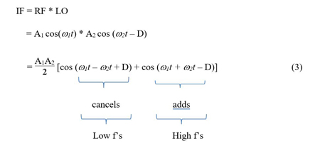
Note that the two frequencies, w1 & w2, are the same.
The resulting equation then becomes:
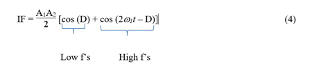
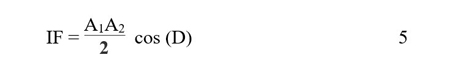
The complete design incorporates a low pass filter, so the high frequency contributions are filtered out. As such, the equation is further simplified:
Assume the delay element, D, is a long length of semi-rigid cable (see Figure 4). A signal incident upon the delay line, which is shown as a cosine, travels down the line and eventually escapes from the other end with a phase that is clearly dependent on length L. Therefore, delay D is a function of length L and can be expressed as D(L).

Figure 4 A wave in a delay line.
Figure 5 shows that for the same length of delay line with two distinct incident frequencies, the phase shifts are considerably different.

Figure 5 Two different frequencies in a length of delay line.
The delay line causes a phase shift as a function of frequency. So, D is a function of frequency and can be expressed as D(ƒ).
Equation (5) can therefore be rewritten as:
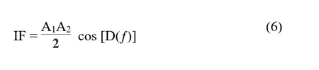
In Equation (5) the frequency contributions of the incident signal cancel and, depending on the amount of delay, the result is a DC value. In Equation (6), however, as the incident frequency changes, the DC value at the output IF changes. This is the desired result and is the basis of the frequency locked loop. As the source frequency changes slightly, the circuit produces a changing DC voltage. The next steps develop how that changing DC voltage is fed back to the source to compensate for frequency drift.
Remaining Unknowns
The circuit in Figure 3 contains the basic elements to “sense” the error associated with the frequency locked loop of Figure 1. However, it remains insufficient for practical applications; there are too many variables and unknowns. To understand the limitations, it is necessary to further explore Equation (6).
Figure 6 is the output of Equation (6) as a function of frequency, showing that the IF voltage varies sinusoidally. For any given voltage, however, frequency is ambiguous, as illustrated with points A and B. These are at the same voltages but located at different frequencies along opposite slopes. If the voltage begins to increase, it is equally likely to be at point A moving to the left or at point B moving to the right (see Figure 7).

Figure 6 Two points with the same voltage.

Figure 7 Two moving points with the same voltage.
Adding an IQ Power Splitter
The circuit in Figure 3 combines a delay element with the basic mixer circuit. The circuit in Figure 8 has two new elements: an IQ power splitter and a second mixer. The excitation source and other elements remain the same.
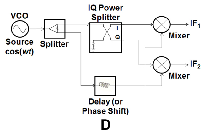
Figure 8 Circuit of Figure 3 with an IQ power splitter and second mixer.
The IQ power splitter gets its name in the following way:
I= in phase (cos)
Q= quadrature (sin)
The term quadrature comes from quad, or four, i.e. four slices of a period. In other words:
¼ λ, where λ is a full wavelength
It is further known that:
An IQ power splitter simply splits a signal in two, one in phase with the source and a second signal 90 degrees out of phase with the source, for short, IQ.
The circuit in Figure 8 is redrawn in Figure 9 and includes some useful equations.

Figure 9 Circuit of Figure 8 with sinusoidal waveforms annotated.
The following can be written:

If the amplitudes (or constants) are appropriately selected, i.e.:
Then Equation (3) can be simplified to:

Similarly:
Selecting amplitudes appropriately such that they become equal to 1, the following is derived:

And, as before, the high frequency contributions are filtered out. The equation can be simplified to:
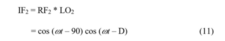
IF2 = cos (D – 90)

The Importance of IF1 & IF2
Figure 10 is a simplified representation of the circuit in Figure 9. If a frequency source is applied, the outputs are two voltages. The voltages are a function of the delay line, which is a function of the source frequency. As the source frequency begins to drift, a change in voltage appears at outputs IF1 & IF2.

Figure 10 Simplified representation of Figure 9.
The significance of the quadrature outputs is that all the variables and unknowns are eliminated. Consider points A & B in Figure 11. The correct location in time is indistinguishable by viewing the voltage of the cosine curve, alone; however, if the voltage along the sin curve is simultaneously monitored, the ambiguity is resolved. For example, if the cosine decreases in voltage and the sin decreases in voltage, then the circuit could only be at location B and moving to the left. There is now a means to sense and quantify the source oscillator frequency drift.

Figure 11 Simplified representation of Figure 9.
THE “COMPENSATION” ELEMENT
The purpose of this circuit (see Figure 12) is to translate frequency drift information into a useful error voltage. For this, the output voltage Verr is calculated.
E is a function of frequency and is arbitrarily defined such that:

The signal at node IF3 is:

Similarly, the signal at node IF4 is:

Verr is then:

Which simplifies to:

Equation (18) when compared with the Equation (14) implies that Verr is equal to zero for all frequencies ƒ. It has thus been derived that Verr is conditionally equal to zero for all frequencies ƒ if Equation (14) is true and E(ƒ) is controlled. E(ƒ) is constructed so that Equation (14) is true and, therefore, Verr = 0.
To tune the VCO (see Figure 1), a control voltage (Vc) is applied. As Vc changes, the VCO frequency should correspondingly change in a predictable and repeatable fashion. If it does not, a resulting error voltage (Verr) is added to correct any deviation. When the VCO frequency returns to its desired value, Verr returns to zero. This all depends upon the function E(ƒ).

Figure 12 Compensation circuit.
The circuit in Figure 12 uses two mixers. As discussed earlier, a mixer is used to multiply two signals. The discussion to this point has been strictly about analog electronics, which been used successfully for many years. However, in the next section, some analog components are replaced with digital components.
The Multiplier
The circuit in Figure 12 is illustrated solely with analog components. There exist available digital counterparts as shown in Figure 13, where a multiplier integrated circuit (IC) and a digital-to-analog converter (DAC) replace the analog mixer. The two signals to be multiplied are applied to Ports X and Y. At Port X, the familiar signal cos [D(ƒ)] appears. The signal at Port Y is supplied by the DAC.

Figure 13 Digital multiplier IC and DAC.
Controlling the DAC
A DAC is a device that takes a digital word and converts it to an analog voltage. In this case, an 8-bit DAC is used. With 8-bits per word, there are 28 = 256 words, where the range is 0 to 255. A sample of DAC output voltages is shown in Figure 14.

Figure 14 DAC input words and output voltages.
If it is desired to produce a sinusoidal signal at Y, then it is only necessary to increment the 8-Bit multiplier DAC digital word between 0 and 255 at a sinusoidal rate (see Figure 15). The analog circuit in Figure 12 can now be realized with the hybrid approach in Figure 16.


Figure 15 DAC digital input versus time (a), analog output voltage versus time (b), output phase versus time (c) and DAC digital input word versus phase (c).

Figure 16 Realized compensation circuit.
The pair of curves in Figure 17 represent the curves for the cos [E(ƒ)] and – sin [E(ƒ)] functions. If a vertical line were drawn through the curves in Figure 17, it would intersect the curves at a pair of points. Figure 18, for example, captures a few obvious pairs.

Figure 17 Multiplier DAC word vs phase.

Figure 18 Several DAC word pairs.
For the circuit in Figure 16, there are two 8-bits DACs. The following questions must be answered: How many pairs of points are possible, what are those pairs and at what phase do those pairs occur? These can be answered with a simple BASIC program. The flow diagram in Figure 19 should be useful; the specific code is left to the reader. There are 1,020 combinations, the first ten of which are shown.

Figure 19 Algorithm to collect DAC word pairs.
PUTTING THE PIECES TOGETHER
Some new elements are introduced in the final design (see Figure 20):
- Verr is fed back to the oscillator and summed with Vc. Vc is the pre-steered voltage to put the oscillator on frequency. Verr is summed back in to correct for frequency drift. Also, a switch is added to the feedback loop to facilitate opening and closing the loop during test and linearization. Ideally, the switch is computer controlled.
- PROMs are added. As DAC words are collected, their values must be stored. External control words direct PROM look-up tables for adjusting the DACs to yield the desired frequencies. The same control word is input at three location ns simultaneously.
- A coupler is added to provide the means to access the signal.

Figure 20 Completed FLL design.
Adding a Delay Line – Discussion of Length
The delay line has some physical length. In Figure 21a there is an image of a sine wave incident on a “short” length of delay line. In this case, the delay line is one wavelength long. Clearly, as the sine wave escapes from the delay line its phase is 0 degrees, i.e. there is zero phase shift.

Figure 21 Delay line length: 1 wavelength (a) and ten wavelengths (b).
If the frequency of the wave increases, its wavelength becomes shorter and the phase of the escaping wave becomes a value greater than zero. For example, the frequency could increase by some amount such that the escaping wave now has 1 degree of positive phase shift. If this were the case, to be useful the detection circuit must be sensitive enough to measure the 1 degree phase shift in order to compensate for it.
If, however, the delay line were ten times longer, i.e. ten wavelengths long (see Figure 21b), the 1 degree of phase shift per wavelength is additive. In other words, the escaping wave will now be shifted by 10 degrees.
As the length of delay line increases, the sensitivity of the loop increases. For locking a loop, this is referred to as the capture window. As the frequency shifts slightly, there is a band of frequencies, or capture window, within which the loop is able to sense and correct for frequency error.
Adding a Delay Line – Discussion of Temperature Stability.
A nice property of a delay line formed from semi-rigid cable is its temperature stability. Because the length of line is important, any change will negatively impact circuit performance. Semi-rigid cable is inherently rugged with regard to environmental conditions, so for most use cases the effect of temperature on electrical length is an insignificant source for error. In extreme environments, however, a thermoelectric heater is sometimes used.
LINEARIZATION
The VCO will not tune linearly without pairing and calibration with the DAC. During linearization, the VCO is swept through its range by the DAC and the resulting frequencies are measured. Because delay lines behave differently at different frequencies, the delay line DACs are also swept through their range. During linearization, the circuit is characterized and digital words are collected. Those digital words are then stored in PROM look-up tables. The calibration steps are summarized below:
- During linearization, the switch in the feedback loop must be open. Otherwise the loop will try to acquire, it will push the oscillator, and the data collected will be erroneous.
- With the circuit running open loop, increment the Vc DAC until the desired frequency is reached. This DAC value will be the first pre-steered value.
- Measure Verr. Of course, it is desired to have Verr to be zero.
- While monitoring Verr, begin sweeping through the cos/-sin DAC values using the using the 1,020 pairs of possible words.
- Continue through these pairs of words until Verr is as close to zero as possible. Since it is sweeping sinusoidally, it will approach zero and begin moving away, so dither it until the best Verr is determined.
- The circuit may be operating at the wrong locking point, as illustrated in Figure 7. It is straightforward to check by simply closing the loop. If the oscillator stays at the proper frequency, then it is at the correct point on the curve. If, however, it tunes off the desired frequency, then the Verr DAC value is incorrect.
- If the Verr DAC value is incorrect, then open the loop and continue sweeping through the set of cos/-sin DAC values until Verr returns to zero with another pair of words.
- Once again check to see if the set of words is correct by closing the loop.
- Once the proper point on the linearization curve is determined, repeat the process through all Vc DAC values required for proper operation. Once the correct point on the curve is found, all subsequent DAC words will be relatively close.
- After all data is collected, program the PROMs.
SUMMARY
A solution to the problem of stabilizing an inherently noisy high frequency oscillator using a delay line employs both analog and digital elements and includes a brief discussion on the software required to control and linearize the final circuit. An advantage of the delay line approach over more common frequency and phase lock loop solutions is the absence of a separate LO. This solution presumes the VCO has some minimum level of stability and then uses itself, delayed in time, as its own reference source. If frequency errors occur, it “senses” and compensates for its own drift. Delay lines realized with semi-rigid cable are relatively stable in most cases and can be environmentally stabilized if necessary. A significant variation is the use of digital elements in place of their more common analog counterparts. The digital elements have less variability, are more standardized and are more cost effective than their analog counterparts.
Biographies
Danny Polidi received his B.S. and M.S. degrees in Electrical Engineering from the California Polytechnic State University, San Luis Obispo, CA in 1990 and 1991. He is currently a PhD candidate in Systems Engineering at CSU. Upon graduation, he started working at Space Systems/Loral on high frequency, microwave designs for space applications. Later, at Radian Technology, he became product manager of the Digitally Tuned Oscillator Product Line where he was responsible for designing new circuits, writing code and production support. At NANOmetrics, Danny managed all electronic engineering activities. From 2004 to present he has worked at Raytheon as a section manager, team lead and cost account manager.
Mike Crist received his B.S. in Computer Science from Embry-Riddle Aeronautical University in 2003 and his M.S. in Electrical Engineering from The University of Texas at Dallas in 2005. He is currently enrolled at Colorado State University working on a PhD in systems engineering. Mike has had a variety of roles over his 20+ year career, including embedded software developer, FPGA developer, circuit card designer, cost account manager, integrated product team lead and engineering tool strategist. He currently works on staff for an Electrical / Mechanical Design Center on various model-based engineering projects.