
Design of an Integrated VNA Covering 70 kHz to 220 GHz
As markets tap higher mmWave frequencies, device and subsystem modeling will follow. These efforts require even higher frequency measurements and equipment limitations that can hinder the development. In addition to standard S-parameters, other measurements such as gain compression, intermodulation distortion and frequency conversion may be needed across wide frequency ranges. Concatenating banded instrument data can work, yet the setup and calibration times become long and, since the uncertainty differs by band, stitching together data sets results in discontinuities.
A broadband vector network analyzer (VNA) covering low frequencies through 220 GHz, with accompanying probes, can resolve many of these measurement complications. Developing such a VNA requires multiplier arrays with adequate output power and control, down-converters with good noise performance and adequate linearity, source and receiver multiplexing that handles wide frequency ranges and a broadband connection enabling a single on-wafer measurement covering the entire frequency range. This article discusses these challenges and the technology options to create a broadband VNA with the required stability, noise, linearity and power performance.
Measurement Requirements
Broadband S-parameters and other microwave measurements are central to many model extraction procedures.1–6 In others, microwave data serves to generate the parasitic elements in the device models. In either case, the quality of the underlying measurement data is important to overall model performance and any descriptive analysis. Further stressing the need for measurement quality, de-embedding is typically necessary to get from the probe tips to the device or subsystem boundaries. Measurements are often required beyond purely small-signal and linear to include compression (AM/AM and AM/PM), harmonics, intermodulation distortion, adjacent channel power rejection and other parameters. Those quasi-linear or nonlinear quantities may be part of a complete nonlinear modeling effort or may be used for basic characterization. Some of these parameters may only be invoked at the subsystem level, with other measurements used at that stage, such as frequency conversion (gain and phase) and modulation distortion. What is common to all is the need to perform the analysis over a very broad frequency range, using an instrument whose own linearity does not dominate the measurement.
Measurement Challenges
Measurements above F-Band (90 to 140 GHz) face several challenges. A typical setup may consist of a broadband system operating to 110 or 125 GHz with banded waveguide modules for the higher frequencies (e.g., 110 to 170 and 170 to 260 GHz or 90 to 140 and 140 to 220 GHz). Mounting and demounting the modules and probes from the probe station - unless one is fortunate enough to have two or three equivalent probe stations - can yield measurement errors.
For broadband device model parameter extraction and IC performance verification, product and process design kit specifications require the same device under test (DUT) to be measured at multiple temperature points (usually five or more), meaning multiple touchdown cycles to the DUT contacts. DUT contact pads suitable for sub-mmWave probing are very small, since parasitic pad reactance increases with frequency. As small pads support only a few RF probe touchdown cycles, measuring the same DUT over the multiple bands covering the whole frequency range and all temperature points may be impossible. This limitation requires engineers to choose different DUTs for different temperatures or frequency bands, which increases uncertainty in the measured parameters and resulting models. A measurement system that reduces the number of touchdowns or enables one touchdown measurements over a wide frequency range will help.
Conventional VNA frequency extenders are sensitive to the measurement laboratory environment. Without multiple feedback control loops, the broadband measurement system characteristics of the remote module can drift faster than those of the base VNA. This leads to more frequent system recalibration, increasing the cumulative measurement cycle time. Frequent system reconfiguration and changeover, required for wide frequency range measurements, increase test cell downtime and risk damaging expensive system components, such as the wafer probes and VNA extenders. This increases the already expensive cost of test.
Data Integrity

Figure 1 Data stitching anomalies occur at measurement transitions between equipment setups.

Figure 2 120 GHz LNA measured at two drive levels, where the nominal level compresses the amplifiers.

Figure 3 Third-order intercept point for two mmWave receivers with the same harmonic number but different LO designs.
Data integrity is also an issue. With several probes used for the different bands - each with unique touchdown characteristics, loss and matching - and several measurement modules used - with different matching, efficiency, spectral purity, stability and noise performance - the data in each band will be measured under different circumstances. While calibration corrects for some of these differences - however, not linearity, noise, spectral purity, drift or repeatability - the uncertainties and distributions in the bands will likely differ. This raises the question of how to handle the inevitable data steps (see Figure 1). The figure shows an example where the uncertainty ranges in two bands overlap; while nothing is fundamentally wrong with either measurement process, the discontinuity complicates the measurement and analysis. If the individual modules and probes have higher uncertainties at the band edges, the analysis becomes even more nuanced.7
Once the measurement data is collected, de-embedding to the desired reference plane can be an adventure. Particularly with BiCMOS and CMOS processes with five to nine metal layers, the desired transistor reference plane may be at the bottom layer and the probe pads at the top. This leads to a “network to de-embed” consisting of many vias and transitions, with significant insertion loss and mismatch.7–9 The increased loss and mismatch complicates the de-embedding process and increases potential error in the measurement results, particularly with drift.10–11 Since such semiconductor fabrication processes are increasingly used at mmWave frequencies, the stability and accuracy of the S-parameter data is critical, which emphasizes the challenges in stitching data and controlling uncertainties in all bands, including touchdown repeatability.
Ensuring Linearity
The RF drive level is important for transistors and amplifiers at these frequencies, as their input compression points may be low. The drive power may need to be −40 dBm or lower and accurate control of the power may be important to avoid inadvertent compression. For quasi-linear measurements, accurate power control is more important.12 The historic solution using a mechanical variable attenuator will not provide sufficient power flatness for this class of measurements. Figure 2 illustrates this, showing the measurement of a 120 GHz LNA where the drive level was not considered (the “nominal” curve). The input power to the LNA was not flat, reaching −15 dBm in places. A second measurement leveled the input power at −40 dBm. The nominal gain measurement shows the amplifier highly compressed, varying significantly with frequency because the drive was not flat versus frequency. While this example may be extreme, at higher mmWave frequencies - particularly with bare transistors - early onset compression is not unusual.
Even if the drive power is accurate, another challenge is the linearity of the instrument receiver; correcting for receiver distortion is difficult. Since many mmWave receivers use relatively high order harmonic mixing, the design of the internal local oscillator (LO) system is important to maintain linearity at the test port. A comparison of the intermodulation performance of two receivers is shown in Figure 3, using free space combining of two tones with 100 MHz separation. The two receivers have the same harmonic number but use different LO systems: one with mild clipping, the other more heavily clipped with active edge sharpening. The residual linearity, expressed as the third-order intercept point of the receiver referenced to the measurement plane, differed by close to 10 dB. As the converter designs have different breakdown voltages, broad conclusions are not possible; nonetheless, a wide variance in receiver linearity can occur in this frequency range.

Figure 4 70 kHz to 226 GHz VNA block diagram (a), showing one measurement setup where the two mmWave modules are connected to on-wafer probes (b).
Broadband VNA Design
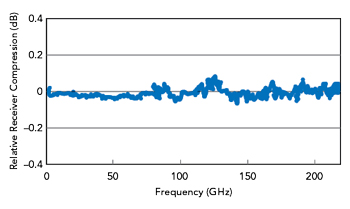
Figure 5 Relative compression of the VNA receiver, showing the difference between +5 and –20 dBm at the VNA port.

Figure 6 VNA power control range at 225 GHz.

Figure 7 VNA stability over 24 hours at room temperature, measured using a thru-line.
One way to address these challenges is using a broadband VNA designed with high linearity receivers and sufficient integration and system control to ensure stability. The block diagram of one such system is shown in Figure 4a, comprising a base VNA and mmWave modules. The module receivers cover 30 to 226 GHz using broadband forward couplers and a high LO sampling system based on III-V nonlinear transmission lines.13 The port referred third-order intermodulation product of these down-converters exceeds 30 dBm, which helps meet the linearity requirements. The modules provide source multiplication above 54 GHz and use a series of four multiplexers, before the measurement couplers, to inject energy from the respective multipliers. Since progressively less power is available at the higher mmWave frequencies, the highest frequency multiplexer is last and has the tightest coupling. Leveling loops for both RF and LO extend to the modules to improve measurement stability.
The integration of the receivers, couplers and multipliers in a small space helps ensure thermal uniformity and stability, as does the close location of the couplers to the probe tip (see Figure 4b). The test port is a novel structure supporting a coaxial mode, using a 0.6 mm outer conductor and a precision UG-387 flange, instead of a threaded body, to form the outer mate. The increased mating area of the flange interface improves durability and significantly reduces the axial forces and bending moments of the connecting device. Repeatability with and without rotation is improved using a precision pin-guided UG-387 flange and limited angular connection orientations, 0 and 180 degrees. Such an interconnect system enables using a single on-wafer probe for measurements from 70 kHz to 226 GHz.
RF wafer probes convert the electromagnetic energy traveling along the three-dimensional media - a coaxial cable or rectangular waveguide - to the on-wafer DUT and its contact pads. This transition is designed to achieve minimal mismatch in the fields and impedance. This is particularly hard to achieve at sub-mmWave wavelengths, so precision wafer probe manufacturing processes are crucial to the overall system performance. Precision probes contribute to well-matched probes for improved calibration and measurement results over a wide frequency range. The 220 GHz MPI TITAN™ Probes incorporate 50 Ω MEMS contact tips to achieve the frequency coverage. Another important aspect of the probe design is maintaining visibility of the tip contacts during touchdowns to minimize potential inaccurate placement. Consistent positioning of the probes on calibration standards and small DUT pads achieves better repeatability and reproducibility, even when used by inexperienced operators. An often-overlooked aspect of probe technology is wear. After multiple probe cycles, the length of the probe tip typically shrinks. However, the unique design of the TITAN probe maintains the RF characteristics after hundreds of thousands of cycles; the lifetime of the probe outperforms the lifetime of comparable probe technologies - even on Al DUT pad metallization - reducing the cost of test and ROI of the test cell.
Using an external stimulus, Figure 5 shows the relative receiver compression at +5 dBm input power relative to a −20 dBm input. This performance is achieved through careful control of the LO waveforms used to drive the sampling down-converters.14 As discussed, power control is an important attribute for accurate measurements. One way to achieve it is with a heterodyne detection circuit feeding a leveling loop with widely adjustable time constants and gain. In this system, a wide control range of approximately 35 dB at 225 GHz (see Figure 6) and generally greater than 40 dB below 220 GHz is achieved with reasonable control linearity.
Stability is important to maximize the time between probe tip calibrations and avoid adding data distortion that complicates model fitting and analysis. Figure 7 shows the transmission measurement of a thru line in the port interface’s coaxial structure over 18 hours at 25°C ±3°C. As expected with temperature variation affecting LO cables, the drift increases with frequency since the LO multiplication factor increases with frequency. As the VNA receivers are used below 30 GHz, the RF cable to the modules (see Figure 4) contributes more at the lower frequency.
Summary
Increasingly, broadband mmWave VNA measurements are needed at higher frequencies, creating measurement challenges: stitching data from multiple bands, controlling power levels and ensuring linearity and stability. An integrated, broadband 220 GHz system with a single connection to the DUT is a simple and elegant approach to address these challenges. The linearity, power control, noise performance and stability of such a system improves measurement accuracy and repeatability.
References
- H. Chen, H. Zhang, S. Chung, J. Kuo and T. Wu, “Accurate Systematic Model-Parameter Extraction for On-Chip Spiral Inductors,” IEEE Trans. Elec. Dev., Vol. 55, November 2008, pp. 3267–3273.
- I. Angelov, K. Kanaya, S. Goto and M. Addasi, “On the High Frequency De-Embedding and Modeling of FET Devices,” 73rd ARFTG Conf. Dig., June 2009, pp. 1–4.
- C. Fager, L. J. P. Linner and J. C. Pedro, “Optimal Parameter Extraction and Uncertainty Estimation in Intrinsic FET Small-Signal Models,” IEEE Trans. Micr. Theory Techn., Vol. 50, December 2002, pp. 2797–2803.
- M. T. Yang, P. P. C. Ho, Y. J. Wang, T. J. Yeh and Y. T. Chia, ”Broadband Small-Signal Model and Parameter Extraction For Deep Sub-Micron MOSFETS Valid Up to 110 GHz,” 2003 RFIC Symp. Dig., June 2003, pp. 369–372.
- D. Williams, W. Zhao, R. A. Chamberlin, J. Cheron and M. Urteaga, “Verification of a foundry-Developed Transistor Model Including Measurement Uncertainty,” 87th ARFTG Conf. Dig., June 2016, pp. 1–4.
- J. Martens, “Parameter Extraction from 110+ GHz S-Parameter Measurements: A Heuristic Analysis of Sensitivity and Uncertainty Propagation,” 2011 COMCAS Conf. Dig., November 2011, pp. 1–4.
- D. F. Williams, A. C. Young and M. Urteaga, “A Prescription for Sub-Millimeter-Wave Transistor Characterization,” IEEE Transactions on Terahertz Science and Technology, Vol. 3, April 2013, pp. 433–439.
- N. Derrier, A. Rumiantsev and D. Celi, “State-of-the-Art and Future Perspectives in Calibration and De-Embedding Techniques for Characterization of Advanced Sige HBTs Featuring Sub-THz fT/fMAX,” IEEE Bipolar/BiCMOS Circuits and Technology Meeting (BCTM), 2012.
- D. F. Williams et al., “Calibration-Kit Design for Millimeter-Wave Silicon Integrated Circuits,” IEEE Trans. On Micr. Theory and Techn., Vol. 61, July 2013, pp. 2685–2694.
- X. Ye, “De-Embedding Errors Due to Inaccurate Test Fixture Characterization,” IEEE Electromagnetic Compatibility Mag., Vol. 1 No. 4, April 2012.
- J. Martens, “Common Adapter/Fixture Extraction Techniques: Sensitivities to Calibration Anomalies,” 74th ARFTG Conf. Dig., Dec. 2009, pp. 1–11.
- L. Galatro, S. Galbano, A. Santaniello and M. Spirito, “Power Control for S-Parameters and Large Signal Characterization at (Sub)-mmWave Frequencies,” 85th ARFTG Conf. Dig., June 2015, pp. 1–4.
- J. Martens, K. Noujeim and T. Roberts, “An Improved Stability Broadband/mmWave VNA Structure,” 77th ARFTG Conf. Dig., June 2011, pp. 1–4.
- J. Martens, “Sub-mmWave and THz frequency Conversion: LO Waveform Control and Sampling Technologies,” 8th ESA Workshop on Millimeter-Wave Technology and Applications, December 2018.