

Switches and Matrices Basics
From “Handbook of RF, Microwave, and Millimeter-Wave Components” by Leonid A. Belov, Sergey M. Smolskiy and Victor N. Kochemasov published by Artech House
RF, microwave and millimeter-wave switches and switching matrices provide a variety of important functions, including:
- Control of frequency, power, various circuit parameters, and circuit configurations
- Modulation of signal phase, amplitude, and frequency
- Antenna duplexing for reception and transmission
- Switching to backup (automatic switchable redundancy) units and channels of data transmission
- Control of the beamforming, scan direction, and other parameters of antenna arrays
- Connection of test signals and measuring equipment for the fulfillment of automated measurements
- Digital control of sources, phase shifters, attenuators, delay lines
- Connection of an input port variety to an arbitrary port from a variety of output ports.
Applications differ, for example, by the level of power, frequency, required switching speed, quantity and configuration of simultaneously switched circuits, external environment, control signals, and packages. Therefore, the assortment of the switching components and technology is manifold.
Fundamentals
In the microwave region, switch development requires the consideration of signal parameters (e.g power, amplitude, phase, noise) in input and output lines or ports, which influence the functioning of adjacent units in ON and OFF states (see Figure 1).

Figure 1. Switching speed parameters.
These parameters change during the switching process from the ON to the OFF state and vice versa. The rise time Trise is the time it takes for the RF signal to rise from 10 percent to 90 percent of the ON level. The fall time Tfall is the time it takes for the RF signal to fall from 90 percent to 10 percent of the ON level. The ON time Ton is the time interval from 50 percent of the control pulse to 90 percent of the ON level. The OFF time Toff is the time interval from 50 percent of the control pulse to 10 percent of the ON level. An ideal switch would have zero Ton and Toff (i.e zero delay and zero rise and fall times) with no accompanying transient oscillation or distortion of the incoming signal, except to gate it on or off at the output.
The transient interval between ON and OFF states may have a non-ideal oscillating character depending on the switching technology and switch construction. In a mechanical relay switch, for example, the position in time of the output signal edge may be delayed in a damped oscillatory manner relative to the edge position of the control signal. This has three contributors: 1) an inductive delay in the coil, 2) the time it takes for the physical movement of its contacts, and 3) the bounce time of the RF contacts.
Additional interfering phenomena can occur for even the simplest microwave single pole single throw (SPST) switch. This is attributed to the response of the input or output on frequency dependent RF reflection, lack of coincidence between the switching moment and oscillation phase, the occurrence of higher order transmission line modes, the dependence of circuit S-parameters upon incident power levels, the oscillating character of transients, and nonlinear transformations of the input signal within the switch.
More complex switches differ by the number of ports and positions. One can describe them in terms of multiport networks for multiposition and matrix switches, i.e.:
[B] = [S][A] (1)
where [B] and [A] are matrices of the output and input circuit, accordingly, and [S] is the scattering (transfer) matrix of dimensions m x n, where m is the number of input ports and n is the number of output ports.
The formula (1) represents an idealized model of a sinusoidal signal passage through a linear circuit with known parameters of waves that are incident upon ports and reflected from them. The matrix coefficients in (1) at each signal frequency are defined by the configuration, dimensions, and internal structure of the switch. Equivalent circuits are typically provided by a manufacturer for performance modeling. This equivalent circuit should satisfactorily describe behavior for frequencies exceeding several times the operating frequency in order to evaluate the impact of higher harmonic signals on the signal spectrum.
For a switch with ohmic contacts, the lower frequency boundary of its bandwidth in an ON condition is direct current (DC). Capacitive switches do not pass the direct current. The upper boundary in an ON condition is defined by spurious circuit parameters introducing transmission losses. In an OFF condition, the upper boundary is defined by spurious capacitance or poor isolation that allows the passing of unwanted signals between the input and output circuits, as well as ohmic losses.
Most switch architectures are reciprocal, their forward and reverse transfer characteristics are identical; however, some models of switches, for example, use ferrite or embedded amplifiers (i. e. nonreciprocal elements) so that the input and output ports cannot be changed.
Simultaneous switching of several input and output ports in a large matrix of switches requires determination of the variety of initial and resulting states and paths. To reduce the number of given combinations, custom software is often used.
The variation of each port’s matching conditions in the ON and OFF states, as well as during transition, is important because it may lead to inadequate circuit performance. In this regard, switching circuits can be complicated in order to minimize the impact from switching transients and to ensure the connection of matched loads to open ports.
Switches have limited power handling capabilities and service life depending upon the switching principle, manufacturing technology and materials, as well as the application. Switching in the absence of incident RF (i.e. “cold” switching), for example, induces less stress for higher reliability and a more prolonged life cycle, while increasing switched current decreases reliability and service life.
Classification and Parameters
RF, microwave, and millimeter-wave switches possess various combinations of properties, configurations and constructions. One can distinguish two-position, multi-position, and matrix switches according to the switching configuration. Variants are shown in Figure 2. The basic function is the connection and disconnection of contacts in a circuit through which high-frequency current flows.

Figure 2. Switch configurations: SPST (a), DPST (b), SPDT (c), DPDT (d); Rotary Transfer 3x120 [1-2; 3-4; 5-6 or 2-3; 4-5; 1-6] (e), Rotary 3-position switch [1-3 or 1-4; 2-3 or 2-4] (f), and SP4T (g).
The simplest mechanical single pole single throw (SPST) switch has two terminals, which can be connected or disconnected (see Figure 2a). With two terminals for the coil, such as a relay there are four terminals in total. The pole may be normally-open or normally-closed when the relay is not energized. Adding another output makes it a single pole double throw (SPDT); one output is ON while the other is OFF (see Figure 2b). This can be extended to an arbitrary number of output ports (i.e. SPNT), where one port is on while the others are off. A double pole double pole double throw (DPDT) switch has two pairs of terminals (ports), equivalent to two SPST switches or relays actuated by a single coil (see Figure 2c). The rotary transfer switch is a variant of the two-position switch with the rotor capable of rotational orientation in one of two orthogonal positions as shown in Figure 2d. In the first position of the rotor the terminals (ports) 1 and 2 and 3 and 4 are connected; in the second position, 2 and 3 and 1 and 4 are connected. This circuit can be used to insert or bypass an amplifier, to change an antenna connection between transmission and reception (Tx/Rx), or to connect two microwave transmitters to two alternative antennas. A similar circuit with three contacts spaced +120 degrees apart (see Figure 2e) is suitable for waveguide realization. To increase the number N of switch positions for SPNT switches one can combine simpler circuits (see Figure 3).

Figure 3. Electrical block diagram of a SP16T fan-out switch.
Switches may be implemented by means such as electromechanical (including reed) relays, solid-state relays, micro electromechanical systems (MEMS), non-reciprocal (e.g. ferrites), as well as manually and through programmable circuits. A relay is an electrically operated switch. Relays are used where it is necessary to control a high power circuit with a low power signal. In electromechanical relays, connection/disconnection is enabled with electromagnets and a mechanical mechanism external to the RF circuit. Vacuum-sealed contacts, which connect/disconnect with the help of the external magnetic-static field, are similarly used in reed relays; here the switching mechanism and the RF conductor are the same. In solid state relays, electrical resistance between input and the output ports is employed. It can be achieved by changing the bias voltage in a semiconductor consistent with the specific technology (e.g. PIN diode, GaAs FET) and the specific circuit structure connection (absorptive, reflective). In MEMS switches a microscopic mechanical electrically conductive strip is formed on the surface of a chip, with one end suspended above a contact. This mechanical actuator moves under influence of controlled electrostatic forces to connect the input and output circuits. Typically, nonreciprocal ferrite switches are those in which the magnetic field direction is changed. Switches with the manual control are typically used in measuring and calibration sets. For a programmable switch, its state is controlled by coded signals from a digital control unit.
Failsafe is a mode of operation in which the switch moves to the closed position when the actuating voltage is applied and always returns to a predetermined position when the voltage is removed. This is typically realized by a return spring within the drive mechanism.
A latching relay has two relaxed (bistable) states. The switch remains in a preselected position whenever the actuating voltage is removed or interrupted, and holds that preselected position until a voltage is applied to move it to another position. This can be accomplished with either a magnetic or mechanical latching mechanism.
Normally open (NO) or “push-to-make” is a mode of operation in which all output ports of the switch are disconnected from the input port until a voltage is applied to maintain a selected position. The switch returns to its open position with voltage removal. A polarized relay remains in the last stable position after disconnecting the control signal. Normally closed (NC) or “push-to-break” can be distinguished according to the state of the circuit. A switch with both types of contacts is called a changeover switch.
Terminated or non-terminated switch modes differ according to the loading of the open circuit. A terminated switch contains in its construction an internally matched load in each output port that ensures a low value of VSWR in both the OFF and ON states (i.e. the port in the ON state is matched to the connecting circuit, while the ports in the OFF state are matched to internal loads).
A self-cutoff option disables the actuator current after actuation. Either a series contact (linked to the actuator) or an IC driver circuit enables the cutoff. This option minimizes power consumption. Pulse latching is a term sometimes used to describe a switch without this feature.
A blocking matrix switch has switches on both the inputs and outputs. Therefore, each input signal can be switched to one individual output port. An example of an application for a blocking switch matrix is a radio and antenna system where each radio is connected to a unique antenna. If an application requires an input to be available to more than one output simultaneously, then a non-blocking matrix is used. Non-blocking switch matrices are used in applications such as multiple- input multiple-output (MIMO) transceivers and satellite station receivers.
Full fan-in and/or full fan-out matrices are characterized by the complete set of connection variants with up-stream and down-stream ports. Inter-channel crosstalk for matrices is a measure of the high-frequency signal leakage from one channel to another. It is the result of stray capacitance, mutual inductance, and leakage resistance between channels.
Low-power, medium-power, and high-power switches are distinguished according to the level of switched power.
An indicator tells the system, at which position the switch is in. Indicators are usually a set of internally mounted DC contacts linked to the actuator.
Parameters
The following are some important performance parameters:
- Operating frequency band, typically defined by boundary values of the input frequency for which the loss in the ON state increases by 3 dB; insertion loss (IL) in the ON state is expresses in decibels.
- Voltage standing wave ratio (VSWR) in each state.
- Isolation of the OFF circuit (in decibels) is the ratio of signal level at the input divided by the output signal level. Isolation, in dB, is a positive number.
- Power handling of the input signal Pmax. By default Pmax is the level of input signal power at which signal loss in the ON state increases by 1 dB. In microwave contact switches the maximal power handling of the input signal may arise due to arcing, and contact heating. In solid-state switches, switching power limitations are related to impedance variations in the active zone of the semiconductor material dependant upon the instantaneous voltage (the sum of the bias and high-frequency voltages). Nonlinear distortion of the passing signal may increase with increasing input power. One reason for limited power handling in RF switches, amplifiers, and waveguides in space applications is the multipactor effect, or secondary electron emission, which can cause device failure.
- Life cycle of microwave switches is defined principally by the technology and functional arrangement of the switching zone. In electromechanical switches, for example, contact wear-resistance may depends on whether switching is provided at low input RF power levels (cold) or at the high power levels (hot). Solid state switches have much longer life cycles without the noticeable degradation of key parameters.
- Signal group delay.
- Type, level and polarity of control signals, e.g. transistor-transistor logic (TTL), emitter-coupled logic (ECL).
- Operating temperature, typically -40° to +85° C.
- Passive intermodulation (PIM) or passive intermodulation distortion is the unwanted amplitude modulation of signals containing two or more different frequencies in a system with nonlinearites. A PIM product is the result of at least two multiple high power tones mixing induced by ferromagnetic materials, junctions of dissimilar metals, metal-oxide junctions, contaminated junctions and loose connectors. A typical input power level for testing passive devices is +43 dBm and if the permitted PIM is -120 dBm, the resulting PIM level is -163 dBc. Common third-order intermodulation is -110 dBc and a low level is -160 dBc.
The general specification and testing methods for switches and matrices are defined in MIL-DTL-55041.
Solid-State Switches and Matrices
A solid-state switch provides the functionality of an electromechanical relay but has no moving components, increasing long-term reliability. Solid-state switches also leverage large-scale semiconductor assembly and automation capabilities for lower cost; and, they occupy smaller footprints (transistors are on microscopic levels), which helps in the design of compact systems.
The characteristics of solid-state switches depend largely on the type of the switching semiconductor element, e.g. positive-intrinsic-negative (PIN) diodes, gallium arsenide GaAs or gallium nitride GaN transistor technology and Schottky diodes.
The maximum frequency fmax of the switched signal, its handling power, and switching speed are the main engineering parameters that determine their performance advantages. The maximum frequency is defined by properties of the semiconductor structure. The power Pmax of input microwave signals for the solid-state switch is characterized (by many manufacturers) with two main parameters: P1dB and PIP3. P1dB corresponds to the input power at which the transfer function decreases by 1 dB compared to its small-signal value. PIP3 is the high-frequency power of the test signal in the form of the sum of two sinusoidal signals, f1 and f2, of equal level at which the level of unwanted combination products of the third order in the output (2f1–f2 and f1–2f2) is equal to the level of the signal at frequencies f1 and f2. A higher number is a measure of the switch’s ability to handle higher input power levels with less output distortion in its ON state. The value of PIP3 for PIN-diode switches exceeds by 5 to10 dB the level of P1dB. Field-effect GaAs transistors can increase this difference to 20 to 25 dB.
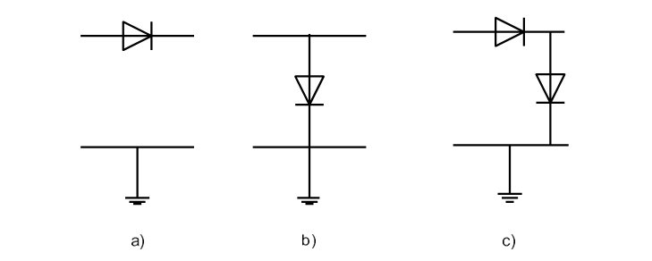
Figure 4. Diagrams of various switch configurations: series (a), shunt (b), and series-shunt (c).
Solid-state switches can be connected in series, shunt, or in combination (see Figure 4), and the resistance of these devices takes is maximal or minimal value depending on bias. Solid-state switches and matrices in the RF, microwave and millimeterwave ranges are offered by many manufacturers.
PIN-Diode Switches
Switch design using PIN diodes can employ shunt, series, or compound topologies. It is usually difficult to achieve more than 40 dB of isolation using a single PIN diode, either in shunt or series, at RF and higher frequencies. PIN diodes can be designed for high power (tens of hundreds of watts) and the multi-octave bandwidths; however, the trade-off is higher loss and lower isolation.
The typical parameters of some models with PIN-diode technology are shown in Table I.


Figure 5. PIN SP24T switch model PSW24-0618-13-11 (Courtesy of Paciwave Inc.).
They differ by physical construction, architecture (e.g. from SPST to SP36T), operating frequency from 0.1 to 40 GHz, absorptive versus reflective configuration, power handling and switching time. Figure 5 shows an external view of a 6 to 18 GHz pin diode SP24T switch. It has 60 dB Isolation, 10 dB IL, 30 ns switching speed, and power handling of 100 mW average/2 W peak).
FET/GaAs Switches

Figure 6. Typical block diagram of a FET switch.
A switching field-effect transistor (FET) is a three port device (see Figure 6), where the channel between source and drain ports forms a conduction path for the RF signal and the gate port controls whether it is blocked or passed. A DC control voltage applied between the gate and channel provides this function. FET switches offer relatively narrower bandwidths, lower power levels (less than 1W), lower loss (less than 0.8 dB), and higher isolation than PIN diode switches.
Manufacturers of solid-state switches use patented solutions for the drivers (logic circuits for the level of control signals to convert from a TTL or CMOS input voltage to the complementary drive signals required for GaAs FET switches with the appropriate operating speed). There are three basic elements in a GaAs FET driver circuit: the TTL input buffer section, a voltage translator, and complementary output buffer stages (see Figure 7). Separate driver’s ICs enable the matching of performance to requirements, such as linearization of the control characteristics. Drivers embedded into an IC provide minimal dimensions and minimal current consumption.
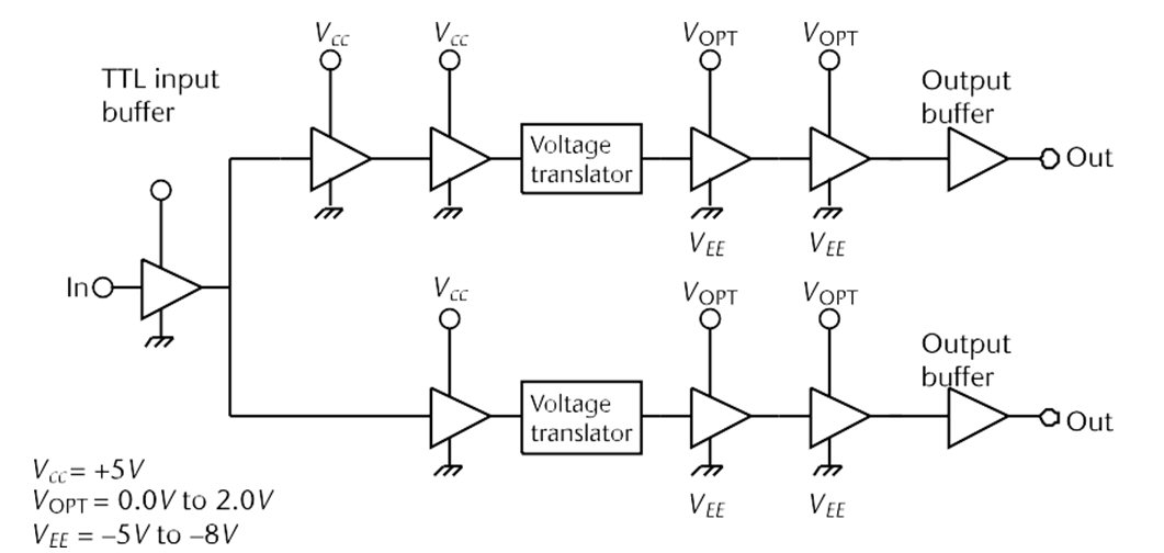
Figure 7. GaAs FET switch driver block diagram (Courtesy of M/A- COM Microelectronic Division).
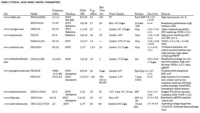
Some parameters of MMIC solid-state switches in GaAs technology are shown in Table II. Solid-state switches using GaN technology are a promising development for high sitching speed switching, high switching power, good OFF-state isolation and low losses in the ON state.
Solid-State Matrices
The full-fan-in matrix topology (see Figure 8a) allows for multiple simultaneous paths and for inputs to share outputs. Input signals are combined into a shared output.
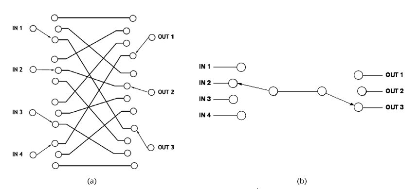
Fig. 8 Diagram of a non-blocking (a) and blocking (b) matrix.
For example, input 2 is routed to output 1, and input 3 is also routed to output 1. Output 1 (or any other output) can be routed to other available inputs. The full-fan-out matrix topology allows for multiple simultaneous paths and allows outputs to share inputs. Full-fan-out matrices are typically used at downlink or receive sites. Full-fan-in matrices are the complement to the full-fan-out topologies, and are typically used at uplink or transmission sites.
The blocking matrix topology (see Figure 8b) limits the number of simultaneous paths in the matrix. Most users will find that this topology is very limited in its capabilities and will not suit their needs. For example, when input 2 is routed to output 3, other paths between other inputs may be blocked. The non-blocking matrix topology allows for multiple simultaneous paths, but no paths may share an input or an output (also known as Fan Out = 1). For example, input 1 is routed to output 3, input 2 is routed to output 2, and input 4 is routed to output 1. At this point, input 3 is unroutable.
Solid-state switching matrices (see Table III) are manufactured as arrays of simple switches within a chip or an integrated microcircuit. Due to the large number (on the order of hundreds) of ports, the quantity of possible combinations of connections can be huge.

Coaxial Electromechanical Switches and Matrices
Coaxial electromechanical switches can be divided into two categories based on their architecture: latching and nonlatching relays. Latching relays are used for applications when long-term latched states are required and switching is not very frequent. Examples for such applications include the antenna switching for redundancy. In this type of application, the receiver/transmitter antenna switching is not frequent as they are either switching for redundancy or only when there is a need to transmit and receive at a different location or frequency.
For momentary switching applications, while performing automated testing, there can be a frequent need for changing the test ports to either switch input test signals or direct output test signals to another port. Nonlatching relays are suited for these kinds of applications, saving time in operation, as de-energizing of a coil is not required. Electromechanical switches are broadband, typically from DC up to 40 GHz. They can also handle high power, on the order of 100 W, over the operating frequency range. Insertion loss can range from 0.2 dB to 0.6 dB and isolation can range from 50 to 90 dB. Switching time is 10 milliseconds and greater.
Electromechanical designs offer better insertion loss, VSWR, power handling, and isolation, but have slower switching times. Tradeoffs are in cost and mechanical dimensions. The cost is involved in machining the parts to certain dimensions, assembling, tuning the relay, and performing final tests. Electromechanical switches have larger mechanical dimensions due to minimum connector spacing requirements for isolation and power handling, magnetic coils, and the separation between them to operate desirably. Key parameters of typical designs are shown in Table IV.

Among additional specifications for electromechanical switches are the following:
• Number of cycles of switching (life cycles).
• Nonsimultaneous switching of several contacts.
• Influence of contact conditions on the value of current passing through them in the switching moment.
• Level of external mechanical vibration and shock (according to stan- dards MIL-STD-202 and MIL-STD-883).
• Usage of pulse latching; self-cutoff, failsafe modes.
• Application of circuit for signaling on the switch status.
• Resistance to moisture, salt atmosphere, thermal shock, solvents.
Furthermore, the following parameters are usually specified:
• Impedance of the input and output circuits (for example, 50 ohms and 75 ohms for coaxial switches).
• Conformity to norms of environmental safety according the used materials.
• Manner of test: hot or cold.
• Circuit for automatic drop into the initial state (the set-reset circuit).
To suppress oscillation in the control coil, which can lead to repeated actuation, shunting arc suppression diodes and actuator damping are used. To suppress switch arcing, some companies use arc suppression diodes.
The lifetime (number of cycles) of an electromechanical switch can be measured statistically on the basis of the increase of average transfer resistance of the closed switch dependance on the number of cycles. It can be on the order of hundreds of milliohms occurring after 10 to 50 million cycles. To increase the life cycle, the manufacturer may use various means such as replacing the springs with electromagnets, choosing more durable and wear-resistive materials, simplifying the construction and decreasing the number of moving parts. Handling power, Pmax, is limited in electromechanical switches by arcing, which decreases with increased operating frequency.
Most electromechanical switches are activated with a relay or a stepping motor. In models with embedded TTL drivers, there is additional circuitry required to match the input logic signals to actuator drive levels. Typical microwave parameters of such switches at 12 GHz are typically VSWR = 1.5:1, isolation of 40 to 60 dB and loss in the ON state of about 0.5 dB.
Waveguide Electromechanical Switches
Waveguide switching devices have less loss in the ON state, increased isolation in the OFF state and can handle a high level of switching power. They function effectively in the millimeter-wave range as well. However, they have a narrow band of operating frequencies and are made of hard metal hollow waveguides. Electromechanical or ferrite circuits for state control are commonly used in such switches.
Parameters of some waveguide switches are compared in Table V. The usual types of waveguide switches are failsafe or latching, and the typical configuration is SPDT or transfer. Losses in the ON state do not exceed 0.05 to 0.1 dB, the isolation of the OFF channel is 60 to 80 dB, and the switching time is about 15 to 20 ms. Switching of continuous wave (CW) average power in waveguide switches is limited by disruption and arcing phenomena in the microwave lines. Pulse power is 20 to 50 times higher than CW depending on test conditions and construction. The typical guaranteed number of switching cycles is no less than 200,000 to 1 million.

Microelectromechanical Switches
Microelectromechanical systems (MEMS) are an attractive alternative to solid-state technologies for the realization of RF switches since they offer low power consumption, improved RF performance, high isolation and linearity, a high degree of miniaturization, and reduced costs. MEMS switches hold an intermediate position between solid-state and electromechanical switches; they are well integrated with the other active semiconductor microwave components while having the advantages of mechanical switches, such as the absence of nonlinear distortion, high DC resistance in OFF states and low loss in ON states. Switching time is a factor of hundreds less than electromechanical switches as well. A great number of serial switching MEMS components (with capacitive or ohmic contacts) are offered and there are publications reporting the development of experimental switches with dimensions on the nano scale, i.e. nano-electromechanical systems (NEMS).
RF MEMS switches are electrostatically actuated cantilever beams connected in three terminal configurations. Their functionality is analogous to a field effect transistor, and the terminals are similarly labeled as source, gate, and drain. The electrostatic force pulls the free end of the beam (the gate) into contact with the drain. When the voltage is removed, the beam acts as a spring, generating sufficient restoring force to open the gate between source and drain, thus breaking the circuit. In multithrow switches, each throw is an independently actuated cantilever. RF MEMS switches provide high reliability, on the order of 100 billion mechanical life cycles which is on par with their solid-state and electromechanical counterparts. They also provide low insertion losses of less than 0.5 dB for frequencies up to 38 GHz. Isolation for a single switch is on the order of 20 dB, but higher isolation can be obtained with a combination of series and shunt switches contained within the same package.
The MEMS switch is usually implemented in a planar microwave construction on a silicon substrate (see Figure 9) created by a metal etching or evaporation process. A flexible metal cantilever has one end permanently connected to the input line. The other end may move under action of a static electrical charge to connect to the output line. After changing the switch state, the control can be eliminated, so that the hold-on current is equal to units of nano-amperes and power consuming by the switch in the hold- on condition is negligible. 
Figure 9. MEMS switch in a closed (a) and an open position (b).

Figure 10. Dual MEMS switch for DC–6 GHz range (size 1.5 x 1.5 mm).
In the ON condition, the contact resistance is equal to parts of an ohm, which leads to insertion losses of hundredths of a decibel at 6 GHz. In the OFF condition there is a break in the transmission line with a capacity of tenths of a femtofarad, which provides isolation on the order of 60 dB. An example of a 6 GHz dual MEMS switch is shown in Figure 10.
The significant advantage of MEMS switches is that they use the same low cost/high volume manufacturing technologies as active solid-state elements and are easily incorporated into multi-function microwave integrated circuits (MMICs). In addition, MEMS technology has its own advantages:
1. Miniature implementation suitable for increasing its upper frequency limit frequency to 50 GHz.
2. Higher ratio isolation to and insertion loss as compared to diode and transistor semiconductor structures.
3. Practical absence of power consumption after contact closing and breaking.
4. High immunity to environmental factors.
5. Greater power handling (up to 30W) compared to semiconductor switches.
6. High static sensitivity voltage (up to 2 kV).
7. High linearity.
8. Fabrication cost less than that of semiconductor switches.
The main shortcoming is a lower switching speed (switching time = 1 to100 microseconds), which also depends on the contact state (i.e. whether the contact is making or breaking). Moreover, for the electrostatic control it is necessary to form the control voltage pulse (40 to 120V), and for magnetostatic control it is necessary to form the current pulse (10 to 100 mA) with duration from 0.5 to 500 ms. This increases the time interval between repeated cycles of switching.
A typical MEMS switch actuated at 20 V achieves better than 22 dB return loss and less than 0.7 dB insertion loss in the ON state from DC to 40 GHz; it provides better than 30 dB isolation in the OFF state. Typical parameters of serial MEMS switches and matrices are presented in Table VI.

Ferrite Switches
Ferrite switches or relays have higher power handling and shorter switching times than electromechanical switches, higher power handling than PIN-diode switches and shorter switching times than rotary electromechanical switches. They may also provide polarization selectivity and directionality through the non-reciprocal properties of the ferrite material.
Some variants of the ferrite waveguide switches are shown in Figure 11. In Figure 11a, a ferrite circulator is used in which the direction of the magnetic field is controlled by a current pulse in the bias coil. In Figure 11b, a T-bridge, two 90 degree ferrite phase shifters and a directional coupler in a Butler matrix configuration are used to construct a toroidal SP2T switch. The T-bridge splits the incident wave into two directions with the same amplitude and phase. The phase shift by +90 degrees directs the output signal power to either the first or second output of the directional coupler. Functionality, which can be added, includes power splitting, polarization, and cascading of individual elements to create switch matrices.
Figure 11. Ferrite waveguide switches based on the principle of switching of polarity of the magnetic in a circulator: spst switch (a), sp2t switch (b).
Reed RELAYS

Figure 12. Reed relay diagram.
A radio frequency reed relay uses an electromagnet to control one or more reed switches. The reed relay comprises magnetically-controlled RF contacts enclosed in a vacuum sealed or inert gas filled container with an external actuating coil and driver circuit (see Figure 12). The voltage required to initially close the relay and the voltage required to maintain it in a closed state are usually expressed as the pull-in and drop-out voltage, respectively. The time from coil de-energization time to contact opening or first contact closure is called the release time. Reed relays switch frequencies up to 10 GHz with powers up to 50 W. Switching times are greater than 50 ms.
Compared to electromechanical and MEMS relays, reed relays have longer lifetimes (up to 10 million cycles). Their advantages in the HF and RF bands are high insulation resistance to typically 1014 ohms and over 200 volts isolation across the contacts. Rise times of 40 picoseconds are typical.
The figure of merit for a reed relay is
RC = pF•ohms (2)
where R is the closed contact resistance and C is the open contact capacitance. The lower this product, the better the high frequency performance; typically for Reed relay RC is approximately 0.02 pF•ohms. The best available solid-state relays currently have pF•Ohm products equal to about 6 pF•Ohms. Reed relays have demonstrated mean time between failures of several hundred million to several billion cycles of closure at typical signal switching levels.
Related Publications
- H. J. De Los Santos, RF MEMS Circuit Design for Wireless Communication, Artech House, Norwood, MA, 2002.
- H. W. Johnson, High Speed Signal Propagation: Advanced Black Magic, Prentice-Hall, Upper Saddle River, NJ, 2003.
- G. M. Rebeiz, RF MEMS: Theory, Design, and Technology, John Wiley & Sons, New York, 2003.
- T. Manning, Microwave Radio Transmission Design Guide, Artech House, Norwood, MA, 2004.
- M. Golio (ed.), RF and Microwave Passive and Active Technologies, CRC Press, Boca Raton, FL, 2008.
- V. Gurevich, V., Electronic Devices on Discrete Components for Industrial and Power Applications, Boca Raton, FL: CRC Press, 2008.
- A. -Q. Liu, RF MEMS Switches and Integrated Switching Circuits (MEMS Reference Shelf), Springer, New York, 2010.
- R. Ghodssi and P. Lin, MEMS Materials and Processes Handbook, Springer, Berlin, 2011.
- US MIL-DTL-55041F, Detail specification: Switches, Waveguide, General Specification for, January 2012.
- B. Yassini, S. Choi, A. Zybura, M. Yu, R. E. Mihailovich and J. F. DeNatale, “A Novel MEMS LTCC Switch Matrix,” IEEE MTT-S International Microwave Symposium Digest, June 2004, pp. 721-724.
- C. L. Goldsmith, D. I. Forehand, Z. Peng, J. C. M. Hwang and J. L. Ebel, “High-Cycle Life Testing of RF MEMS Switches,” IEEE MTT-S Internatinal Microwave Symposium Digest, June 2007, pp. 1805-1808.
- D. Gotch, “A Review of Technological Advances in Solid State Switches,” Microwave Journal, Vol. 51, No. 11, November 2007, pp. 24-34.
- M. Daneshmand and R. R. Mansour, “Redundancy RF MEMS Multi-Port Switches and Switch Matrices,” IEEE/ASME Journal of Microelectromechanical Systems, Vol. 16, No. 2, April 2007, pp. 296-303.
- K. Y. Chan and R. Ramer, “A Novel RF MEMS Switch with Novel Mechanical Structure Modeling,” Journal of Micromechanics and Microengineering, Vol. 20, No, 1, January 2010, pp. 1-9.
- T. Boles, and A. Freeston, “New Nanosecond Switch Technology,” Microwave Journal, Vol. 54, No. 6, June 2010, pp. 56-60.
- P. Hindle, “The State of RF/Microwave Switches,” Microwave Journal, Vol. 54, No. 11, November 2010, pp. 20-36.
- J. Hueso, D. Raboso, D. Schmitt, V. E. Boria, B. Martinez and C. Vicente, “Study of the Multipactor Effect in Bandpass Wedge-Shaped Waveguide Filters,” IEEE Transactions on Electron Devices, Vol. 58, No. 9, September 2011, pp. 3205-3212.