I first realized there was a major problem in 1982 when I moved from GE Valley Forge Space Division to GE Electronics Laboratory (E-Lab) in Syracuse to design some of the first GaAs monolithic microwave integrated circuits (MMIC). I took over the design of a C-band low noise amplifier (LNA). I was told that my first design had to work; there was no budget or time left for any more wafer fabrications. The previous design was compact and made extensive use of spiral inductors. However, the spiral inductors were almost complete unknowns and as a result the previous design did not work.
Fortunately, I could make the chip as large as I wanted to. So I changed all the inductors to equivalent transmission lines and made sure they were spread out so there was very little stray coupling. The design worked the first time. However, the chip area was about 3 mm by 6 mm, and it used only two transistors. This was acceptable for a first of its kind, but it was clear we had to do something so that we could reliably design compact MMICs in the future.
Making this problem even clearer was effort on other, size constrained MMIC designs. We were doing multiple iterations on these chips. At US $50,000 and three to six months per wafer fabrication, the situation had to change or GaAs MMICs would end up in the technological trash bin of history, just another blue-sky research project that no one could reduce to practice. This is when I, and several other researchers, turned to numerical electromagnetics for the answer.
Early Microwave Design
In the early 1980s the main microwave design tool was the Smith chart. The IBM-PC was introduced in 1981 (4.77 MHz, 16 kb RAM, no hard drive), and it would be several years before serious microwave design software would be available, and then even longer before it was widely accepted. The most significant commercial circuit theory tool seeing active development at this time was on mainframe computers, although it too had not yet realized widespread acceptance. At E-Lab, we used circuit theory software I had written at Space Division; it ran on a VAX computer that occupied a large air-conditioned room. (I understand that the software was actually still in use in some locations as recently as a few years ago.)

Fig. 1 The author dveloping analysis software on Apple computer in 1983.
In addition to the circuit theory software I had written on the VAX, I had also, on my own time, written a nice little antenna analysis program, Annie, on an Apple™ computer (see Figure 1). Lacking a compiler, I wrote the entire program in assembly language, including a full set of floating point arithmetic routines (no floating point coprocessor). I sold over 250 copies of that program to radio amateurs. A friend sold another 250 copies in Japan. The PC version of the program still works and is still available.
Given that simple circuit theory microwave software was not yet well accepted and computers were very limited, it was quite a jump to go all the way to numerical electromagnetics. Electromagnetics was viewed by microwave designers as a totally useless academic exercise yielding lots of PhDs, but little or nothing in the way of timely applied solutions. The Smith chart and the Exacto knife were far superior. At that time, microwave designers were completely correct.
Of course, the Exacto knife did not work for GaAs MMICs. Several far-sighted researchers, myself included, saw this and proceeded to explore potential solutions, especially for planar circuits. One such technique is the method of moments. I was fortunate in that the originator of the method of moments, Professor Roger Harrington, taught at Syracuse University, just a 10-minute drive from E-Lab. I wasn’t sure exactly how, but I had a feeling that the method of moments had some possibilities. I decided it was time to go for my PhD degree under Professor Harrington. My future was set.

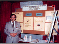
Fig. 2 The author's first publication in 1987 of the EM technique that he commercialized.
Figure 2 shows the open forum paper (IMS 1987, Las Vegas, NV) where I first presented the method of moments approach I eventually commercialized. That was an especially hectic time for me, as I was also the open forum chairman.
Other researchers doing planar EM work at this time included Rolf Jansen, Achim Hill, Larry Dunleavy, Jian-X Zheng, Joseph Pekarek, Y.L. Chow, Niels Fache, Juan Mosig, Robert Jackson and others. Work from all of these researchers influenced the entire field, and some actually made the very considerable jump to commercial products.
By the end of the 1980s, circuit theory was well embedded in the microwave design flow and EM was just getting started. By the end of the 1990s, EM analysis was firmly embedded, too. Thus, we refer to the 1980s as the decade of circuit theory microwave design, and the 1990s as the decade of EM-based microwave design.
Commercialization
Making the jump from academic research to successful commercial product deserves discussion. In my own case, having grown up as a farm boy pitching hay and a driving tractor, I could not even spell entrepreneur, much less consider becoming one. So I tried everything I could short of commercializing the software myself. I went to all the major EDA vendors and actually had strong interest from two of them, but both eventually turned me down. I went to the companies that had funded my PhD research; it was not in their overall corporate strategy, a reasonable objection. So, I either had to commercialize it myself, or drop it and get on with life.
From selling the Annie program, I knew commercialization was going to be way too much work, so I decided to drop it and get on with life. I decided to pursue an academic career. Maybe I could do more development as part of my research and eventually someone might pick up the software. I did successfully obtain a temporary position at Syracuse for two years, but serious attempts applying for tenure track positions at both Syracuse and Cornell failed. So, in between teaching courses, I spent those two years preparing software for applied use and then I would “quit my day job.” It was like I was being forced to become an entrepreneur.
Looking back on the effort to commercialize the software, I subjectively estimate about 10 percent of my total effort has been in doing the underlying EM theory and numerical software. Another 30 percent was spent doing productization, putting the software into a form that could be used in applied work. This includes setting up substantial automated testing, writing documentation and developing a good user interface. About 60 percent of the total effort has been in marketing and sales.

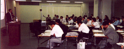
Fig. 3 An EM seminar in Tokyo in 1995 captures a large audience.
A portion of the marketing and sales was simply traveling all over the world to tell skeptical microwave designers about the wonders of numerical electromagnetics. Figure 3 shows the strong interest my seminars generated, this one in Tokyo, Japan, in 1995.
Occasionally I hear researchers complaining that they publish research and someone else gets rich. My reply is that if they want to get rich, just do the productization, marketing and sales as described above and you too will become wealthy... maybe. I chose (or perhaps was forced) to take the commercialization route. This turned out to be successful, but I fully realize that in doing so I have not experienced research and publishing in more depth and in a wider variety of topics. I sometimes wonder what my life course would have been if I had been successful in one of my tenure track applications, but that I will never know.
Also, I occasionally get enquires like, “I have this really neat EM code, it’s 90 percent done and only 10 percent is left to do, would you like to sell it?” I reply that they have the right numbers, but in the wrong order. Most researchers leave it there (just like I tried to do), but every now and then one takes up the challenge and puts in the extra 90 percent required to commercialize. I have heard essentially this same story from several microwave software vendors.
Electromagnetic Theory
Don’t worry, no equations here. If you want equations, there are lots of papers you can go read. Here you will get a simple, equation-free, high level understanding.
There are two basic approaches to the method of moments as applied to planar circuits. In the approach I use, we place the problem in a rectangular, shielding box. When we work the equations, we view the sidewalls of the box as a rectangular waveguide propagating in the vertical direction. The top cover and bottom ground plane are just waveguide terminations.
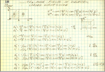
Recall that the M and N, TE and TM waveguide modes all have cosine and sine terms in them. In applying the method of moments, we write the fields as a sum of these waveguide modes. This is a sum (over all M and N modes) of cosines and sines. What is a sum of cosines and sines? It’s a Fourier series. Thus, we can use a 2-D fast Fourier transform (FFT) to sum all these cosines and sines. Figure 4 shows a portion of a page from my notebook where I calculated these sines and cosines at the beginning of my PhD research. While the equations can fill pages, the basic ideas are simple.

Fig. 4 A page from the author's PhD notebook showing the sines and cosines of the waveguide modes summed by the FFT.
Using an FFT like this in EM analysis has an important disadvantage that is identical to the disadvantage in using the FFT in signal processing. If you have a time signal and you want to do an FFT, the first thing you do is to uniform time sample the signal. In FFT-based EM analysis, the first thing you do is uniform space sample across the surface of the substrate. Thus the circuit analyzed is snapped to a fine uniform underlying FFT mesh. Fortunately, the FFT is so fast that this mesh can easily be 1000 by 1000 cells, which means FFT cell size can be as small as a pixel on a computer screen.
The advantage of using the FFT is that all coupling between all cells is quickly calculated to full numerical precision. This results in very high accuracy and a typical dynamic range of 100 to 180 dB. This advantage is identical to the high dynamic range provided by audio CDs. If you must meet an 80 dB filter rejection specification, it is easy to do using FFT-based analysis.
The second planar method of moments approach assumes an unshielded environment. Now, a numerical integration must be used to calculate the fields. The advantages and disadvantages of this approach nicely compliment the FFT approach. The advantage is that the numerical integration may be performed over any limits, thus subsections can be triangles or rectangles of any size. The disadvantage is that numerical integration is slower than an FFT for a given subsection count and that numerical integration error reduces dynamic range.
Ideally, a designer should have access to both types of analyses. The experienced designer can effectively enjoy the advantages of both approaches. For given circuit and accuracy requirements, one tool might be preferred over the other. In cases where high probability of success is critical, circuits should be analyzed using both approaches and any differences fully understood.
For example, if a circuit is to be used in an unshielded environment, an unshielded analysis is generally appropriate. If you want to quantitatively evaluate the significance of surface wave coupling to nearby components, then analysis with a 3-D volume meshing tool including the specific nearby components is typically required.
If only the general importance of surface wave coupling is desired, an unshielded analysis by itself is difficult to use. This is because the effects of surface waves tend to be smooth with frequency and their existence is not easily discerned by just viewing the S-parameters. In this case, a shielded analysis should be applied. If a circuit generating strong surface waves is placed in a shielding box, then the surface waves become easily recognized box resonances. If you see numerous box resonances in the shielded analysis, you can be confident that the actual unshielded circuit has a strong likelihood of surface waves and undesired coupling to nearby components.
If high accuracy is required for a filter in a shielding box, a shielded EM analysis must be used and the box set to the same size as in the actual circuit. A filter’s enclosure and environment can have a strong and sometimes unexpected influence on the filter response.
Shielded analyses can approximate an unshielded environment and unshielded analyses can approximate a shielded environment. However, in each case, due to accuracy and speed issues, if both types of analysis are available, the appropriate native environment is preferred.
There are numerous volume meshing EM tools available. Most are based on or related to either finite elements or finite difference time domain. Typically, unless there is some kind of 3-D arbitrary attribute to the circuit (as in the stray coupling to external components example above), such analyses should not be used for planar circuits. Analysis times can be substantially longer than for a native planar analysis. While such analyses typically give a reasonable indication of the correct result, very high accuracy can be difficult to realize.
To get a quick indication of accuracy, just look at the current distribution. For example, accurate calculation of I2R loss requires an exceptionally accurate evaluation of S-parameters. This is because planar circuits naturally have very high current on all edges. Confining a large portion of the current to the edges significantly increases loss. In order to accurately calculate I2R loss, this high edge current must be accurately calculated. This, in turn, requires an exceptionally fine mesh right at the edges of all lines. This makes any volume mesh so fine that it is difficult to analyze. In contrast, volume meshing approaches tend to work well for 3-D arbitrary structures where planar approaches have difficulty.
Planar EM tools mesh only the metal of a circuit, not the volume. Typically, they can automatically and efficiently generate a fine mesh on edges, allowing accurate evaluation of the high edge current. For some tools, such “edge meshing” is default, in other cases it must be manually invoked. If high accuracy is required, edge meshing must be used. As an added benefit, when edge meshing is used, adaptive meshing is unnecessary. In fact, most planar EM tools do not even bother including an iterative adaptive mesh.
Whenever high accuracy is needed, and no matter what EM tool is being used, always view the current distribution for at least one or two frequencies. The current distribution must be smooth, physically reasonable and have high edge current. All of these characteristics are absolutely required if high accuracy results are to be realized.
Another excellent check for accuracy is to perform a convergence analysis. This is easily done for any EM analysis; just keep making the mesh finer and finer. For example, if an initial analysis uses a mesh size of 20 subsections per wavelength (the minimum that should ever be used), repeat the analysis with 40, then 80 and then 160 subsections per wavelength. For FFT-based analyses, just keep cutting the cell size in half. Plot the results. You should see a clear convergence, with the difference between each set of curves (no matter what it is that you are plotting) reducing by about half each time you refine the mesh. If the difference remains constant, or if the difference starts increasing for finer meshes, the situation must be resolved or the design is at risk.
Also keep in mind that accuracy depends not only on the number of subsections per wavelength, but also on the size of the subsections with respect to current variation on the metal. This is why high accuracy requires narrow subsections at the edge of lines to adequately represent the high edge current. If thickness is important, multiple subsections through the thickness of the line can also be important.
Characteristic What?
When I first started working in numerical EM, most (of the very few) users had a good solid knowledge of microwave design. Over the years, with a few fortunate exceptions, many universities have dropped or compromised their EM and RF design courses. Perhaps they felt all that RF stuff was old fashioned and they wanted to work on modern topics. After all, Maxwell’s equations are over 100 years old. Traveling waves and characteristic impedance are terribly complicated. All this is just a useless holdover from a by-gone era.
Suddenly, wireless is a hot topic. These universities are only just now realizing that they should at least maintain and maybe even increase their attention to RF design. In the meantime, I have seen a strong increase in the number of “RF designers” who have been almost literally dumped into the field with little or no preparation. We help them out as much as we can. Fortunately, most of them are receptive, but we are no substitute for a good solid academic grounding in EM and RF design.
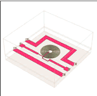
Take, for example, silicon RFIC design. It is common for foundries to measure a large set of components to facilitate the use of their process. Each component is fabricated with a “ground cage” (see Figure 5). The component is measured in coplanar waveguide (CPW), the ground cage strips forming the ground strips of the CPW.

Fig. 5 A typical ground cage.
For true CPW operation, if one amp of current goes into the signal line (the center contact), then one-half amp of current must come out of each of the two ground strips. The ground return currents are exactly balanced. The CPW characteristic impedance and velocity of propagation depend on balanced ground return current.
However, if the ground strips are not symmetric, the ground return current will also not be symmetric, one ground return path having lower reactance than the other. In measurements, this compromises the probe calibration as the probe characteristic impedance and velocity of propagation was calibrated assuming true CPW (balanced ground return currents) operation. Such error is reduced if the probe’s ground strips are shorted together very close to the tip, but the error can still increase to significant levels at a sufficiently high frequency.
In addition, if yet another ground return path is used (the chip ground plane, or worse yet, the silicon substrate itself, for example) when the component is actually used in a circuit, different results (at high enough frequency) will again be obtained. Inexperienced designers forget that the ground return current is very real and is fully half of the circuit being analyzed. At sufficiently high frequencies and for certain circuit configurations, the designers will find themselves confronting old fashioned “ground loops” generating truly bizarre responses.
To make matters worse, inexperienced RF designers often perform their measurements using a manufacturer-provided calibration kit, usually on alumina, and then make their measurements on silicon. This works at lower frequencies, but at high frequencies, where the exact probe tip discontinuity is important, significant error can be introduced.
When there are differences between measured and calculated results, the inexperienced designer is strongly tempted to blame the problem on the analysis software, materials and measurement equipment. However, the problem is actually defective design and measurement technique. This makes life hard for those of us who provide the software, materials and equipment. I am encouraged that this situation should gradually change as universities provide better-trained RF design professionals. In just the last month I have become aware of two major engineering universities starting up new RF design curricula. This transition can occur faster if those of us who are experienced in RF design take extra effort in helping new comers on board.
Interoperability
As you might surmise from the above discussion, in order to be competitive when faced with a wide variety of problems, a well equipped high frequency designer requires multiple EM tools. If best-in-class is desired for each tool, these tools will come from multiple vendors. In this case, interoperability in a heterogeneous EDA vendor environment is critical.
I mentioned that the 1980s was the decade of circuit theory, and the 1990s was the decade of EM-based design. What is the theme for this decade? In my opinion, it is interoperability. At the beginning of this decade, even basic interoperability between a framework vendor’s own tools was a developing situation. Interoperability between multiple vendors was almost non-existent and sometimes even actively discouraged by “total solution” framework vendors.
In just the last several years we have seen significant interoperability arise, even between vendors who are to some degree competitive. I have been personally involved in four such substantial framework integrations. Each of these vendors has tools that are at least somewhat competitive. Why would they want to actively facilitate interoperability to a competitor? It is because they do not want to ever reply in the negative to a customer asking, “I need to use ABC software. Your competitors interface to it. You have a good interface to it too, don’t you?”
In fact, I feel that interoperability is so important that by the end of this decade this issue alone will determine the success or failure of any and all frameworks in the high frequency EDA field.
Closing Comments
I have been involved in high frequency EDA for over a quarter century. I have seen, and had the extreme pleasure of participating in the field of applied high frequency numerical EM analysis from the very beginning. One thing I really treasure and I think is very special is how well the practitioners of our field get along together. I can walk up to nearly anyone in any company and say, “Hi,” and really feel good about it. In sharp contrast to the much larger non-RF EDA field, where business-as-usual lawsuits are common, lawsuits between competitors in our field are extremely rare and generally inappropriate. Yes, we all compete vigorously and now and then we have to posture and bluster, but we all get along together, too. This is important for the designer, because the interoperability that results is much greater and of higher quality. Even though we compete, when it is important for the designer, we also cooperate. And the designer wins.
