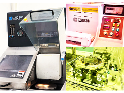
Sensera Inc. is pleased to announce it has acquired and qualified additional thin-film processing equipment including a dicing saw, a wafer bonder and an electroplating cell to meet the growing customer demand in this segment.
"We are very pleased to be able to expand our production capabilities, closely aligning ourselves with growing customer demand. This new production equipment substantially broadens our existing tool set and enables greater vertical integration and process control," said Tim Stucchi, GM/COO of the Sensera MicroDevices Division.
The new dicing saw operates in either fully-automatic or semi-automatic mode for full wafer and custom cuts, featuring a positional accuracy down to 1 μm and a cutting speed of 300 mm/sec. It supports small pieces and allows for custom shaping of silicon, sapphire, Pyrex, quartz, ceramics and metals.
Operating under high vacuum, precisely controlled temperature and high-pressure conditions, the new wafer bonder facilitates extremely demanding applications. Eutectic, thermal compressive, adhesive and anodic bonding processes with a wafer alignment accuracy of 2 μm have been smoothly integrated into Sensera's qualified processes, thus enabling the company to offer many wafer level packaging (WLP) solutions to its current and future customers in multiple applications and market spaces:
- Microfluidic devices for bio-analysis, medical research and drug development
- Pressure sensors for human implantable surgical devices
- Precision accelerometer and gyroscope devices for geo-positioning
- Micro-mirror devices for laser based Automotive self-driving applications
The wafer bond chamber is configurable to process small coupons (from ~10 mm2) and wafer diameters from 25 mm (1 in.) up to 200 mm (8 in.).
The electroplating cell is able to plate and electroform wafers or discreet parts up to a size of 200 mm (8 in.). Typical applications include MEMS, Integrated Circuits (IC) on Si, GaAs and similar glass-type substrates. Sensera's qualified processes achieve exceptionally low residual stress and enable tight thickness uniformity control.
"To drive down cycle times, improve quality control and reduce costs, our fab requires ongoing capability upgrades," stated Ralph Schmitt, CEO of Sensera Inc. "Our objective here is to bring previously outsourced processes back in-house and to expand our internal capability to develop and produce complex MEMS products and solutions. The new dicer, bonder and electroplating cell are just some of the essential steps required to enable innovative development programs and commercial volume customer shipments.”

