
CHANNEL COMPENSATION MODELING
Frequency-dependent I/Q imbalance is modeled to compensate for an imperfect channel. I/Q imbalance compensation modeling is separated for the receiver and transmitter channels.
Receiver Channel Compensation Model
In the receiver, TDC amplitude and phase for the wideband channel are extracted by constructing an orthogonal and cyclically symmetric signal. Wideband time domain modeling is performed by using compensation values for different frequency bands. The real and imaginary parts of the test signal satisfy

where E{} is the mathematical expectation signal. After obtaining α and φ, we solve the inverse matrix of Equation 13 to obtain a frequency-independent TDC expression for the receiving channel.

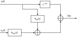
Figure 3 Wideband compensation model for the receiver.
The wideband compensation model (see Figure 3) can be regarded as a combination of the corresponding compensation coefficients for each frequency point. From Figure 3, the expression for compensation can be written as
where hRIf(z) and hRQf(z) are the I/Q channel compensation functions. They are implemented using a finite impulse response (FIR) structure. In Figure 3, the z-N/2 block eliminates the delay of the I and Q paths, and N represents the FIR order.
Transmitting Channel Compensation Model
Because the imbalance of the transmission channel is caused mainly by the physical circuit, external interference is very small. Therefore, the imbalance of the transmit channel is much flatter than that of the receiving channel. In order to compensate for a wideband transmit signal, we use a derivation based on polar coordinates (see Figure 4).

Figure 4 Polar coordinate model for transmitter channel compensation.
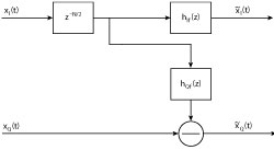
Figure 5 Wideband compensation model for the transmitter.
Assume the I path offset angle is φ. From Figure 5, the relationship of and x̃I and x̃Q (compensated output) with the ideal input signal is

Extended to a frequency-dependent compensation expression,

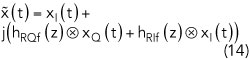
where hSIf(z) and hSQf(z) are the I/Q channel compensation functions. They are implemented using a FIR structure. The z-N/2 block eliminates the delay of I and Q paths, where N represents the order of FIR. Compensation is performed in the baseband I and Q paths.
VALIDATION AND EXPERIMENTAL RESULTS
First, the compensation effect of the transceiver channel was verified, followed by verification of the DPD effect on the signal before and after transceiver channel compensation. Figure 6 shows the software and hardware architecture of the DPD platform. Validation used 20 MHz single-carrier and 60 MHz three-carrier LTE signals with peak-to-average power ratios (PAPR) of 7.25 and 9.29 dB, respectively. All original signals generated in MATLAB were fed to the PA through an FPGA.
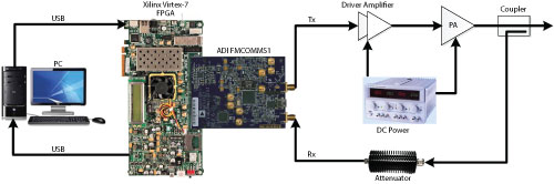
Figure 6 Software and hardware architecture of the DPD platform.
A PA designed with a Wolfspeed (Cree) CGH40010 transistor was used for the device under test. The PA was biased with VGS = -2.7 V and VDS = 28 V, placing the amplifier in class AB mode of operation. The PA was driven to saturation with a peak output power of 40 dBm. The operating frequency band was 1.7 to 2.6 GHz, with DPD validation at 2.4 GHz.
The DPD platform consisted of a Xilinx Virtex-7 FPGA on an ADI RF board. The digital-to-analog converters (DAC) and analog-to-digital converters (ADC) had 16- and 14-bit resolution, respectively. The maximum sample rate of the ADC was 250 MSPS, and the maximum sample rate of the DAC was 1 GSPS.
Effect of Loop Compensation
AM/AM and AM/PM are used to characterize channel memory and nonlinearity. To verify the channel compensation model, the 20 and 60 MHz signals are used to test nonlinearity and memory level with and without the channel compensation model. Measured results for the AM/AM and AM/PM characteristics of the channel are shown in Figure 7.

Figure 7 Measured AM/AM and AM/PM for 20 MHz single-carrier (a) and 60 MHz three-carrier (b) LTE signals.
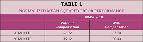

Figure 8 Measured PA output spectrum for 20 MHz single-carrier (a) and 60 MHz three-carrier (b) LTE signals.
I/Q transceiver channel imbalance causes significant signal amplitude and phase distortion in an uncompensated channel. With increased bandwidth, imbalance and resulting distortion are greater. The compensation scheme effectively reduces this distortion. Table 1 compares NMSE performance with and without compensation, showing improvements of 10.9 and 11.3 dB, respectively, for the 20 and 60 MHz LTE signals.
DPD Measurement Results
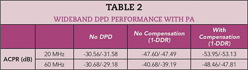
In general, DPD performance depends on the quality of the model and the accuracy of the parameter extraction process. The TDC model described extracts the PA output signal accurately. To verify that it is suitable for wideband DPD, two sets of measurements were made.
Without loss of generality, the measurements were made using the first-order DDR model. Memory depth and nonlinear order number were consistent in the measurements to objectively demonstrate the advantages of the model. Figure 8a shows the results of PA linearization for 20 MHz single-carrier LTE signals. It can be seen that the TDC model has good adaptability to frequency-dependent I/Q imbalance, resulting in better linearization performance in terms of ACPR at the output of the PA. Figure 8b shows the results of PA linearization for 60 MHz three-carrier LTE signals. With the increased bandwidth, the I/Q channel is more sensitive to DPD performance. Table 2 shows measured ACPR performance for the two bandwidths.
CONCLUSION
Wideband channel compensation is becoming more important in communications systems. In this paper, a method of TDC for frequency-dependent channel imbalance in wideband DPD systems is described using the FIR structure in FPGA hardware. Better than 6 and 8 dB ACPR improvement was achieved with 20 and 60 MHz LTE signals, respectively, compared to performance without channel compensation.n
References
- M. Nakayama, K. Mori, K. Yamauchi, Y. Itoh and T. Takagi, “A Novel Amplitude and Phase Linearizing Technique for Microwave Power Amplifiers,” IEEE MTT-S International Microwave Symposium Digest, May 1995, pp.1451–1454.
- Y. Ma, S. He, Y. Akaiwa and Y. Yamao, “An Open-Loop Digital Predistorter Based on Memory Polynomial Inverses for Linearization of RF Power Amplifier,” International Journal on RF Microwowave Computer Aided Engineering, Vol. 21, No. 5, September 2011, pp. 589–595.
- A. Zhu, J. C. Pedro and T. J. Brazil, “Dynamic Deviation Reduction-Based Volterra Behavioral Modeling of RF Power Amplifiers,” IEEE Transactions on Microwave Theory and Techniques, Vol. 54, No. 12, December 2006, pp. 4323–4332.
- L. Anttila, P. Händel and M. Valkama, “Joint Mitigation of Power Amplifier and I/Q Modulator Impairments in Broadband Direct-Conversion Transmitters,” IEEE Transactions on Microwave Theory and Techniques, Vol. 58, No. 4, April 2010, pp. 730–739.
- Y. D. Kim, E. R. Jeong and Y. H. Lee, “Adaptive Compensation for Power Amplifier Nonlinearity in the Presence of Quadrature Modulation/Demodulation Errors,” IEEE Transactions on Signal Processing, Vol. 55, No. 9, September 2007, pp. 4717–4721.
- V. Rampa, “I/Q Compensation of Broadband Direct-Conversion Transmitters,” IEEE Transactions on Microwave Communications, Vol. 13, No. 6, June 2014, pp. 3329–3342.
- K. Rawat, M. Rawat and F. M. Ghannouchi, “Compensating I–Q Imperfections in Hybrid RF/Digital Predistortion With an Adapted Lookup Table Implemented in an FPGA,” IEEE Transactions on Circuits and Systems II: Express Briefs, Vol. 57, No. 5, May 2010, pp. 389–393.
- A. Zhu, J. Dooley and T. J. Brazil, “Simplified Volterra Series Based Behavioral Modeling of RF Power Amplifiers Using Deviation Reduction,” IEEE MTT-S International Microwave Symposium Digest, June 2006, pp. 1113–1116.
- C. Crespo-Cadenas, J. Reina-Tosina and M. J. Madero-Ayora, “Volterra Behavioral Model for Wideband RF Amplifiers,” IEEE Transactions on Microwave Theory and Techniques, Vol. 55, No. 3, March 2007, pp. 449–457.
- G. Xu and T. Liu, “Generalized Two-Box Cascaded Nonlinear Behavioral Model for Radio Frequency Power Amplifiers With Strong Memory Effects,” IEEE Transactions on Microwave Theory and Techniques, Vol. 62, No. 12, March 2007, pp. 449–457.