Advances in GaAs MESFET technology require accurate large-signal MESFET models to correctly predict the circuit performance of power amplifiers and oscillators utilized in RF applications and communication systems. New devices such as PHEMTs and pulse-doped MESFETs utilize a concentrated carrier region in the active layer. This leads to more uniform transconductance behavior versus gate voltage changes and demonstrates a contraction of transconductance when the gate is positively biased. Typically, with these devices, the drain current is limited by the total number of carriers in the channel, not by the forward gate current that may be increasing exponentially with the gate voltage when it is positively biased with respect to the source. The unique IV curve features of pulse-doped devices are shown in Figure 1 by a set of curves taken from an advanced pulse-doped MESFET using the pulsed IV technique.1 A pulsed IV measurement system,2 developed in-house, provides the measurements needed for accurate modeling. Widely used models3–6 cannot adequately predict these curves, and thus fail to simulate the large-signal RF performance of these devices correctly. When applied to circuit simulators such as MWO from AWR or ADS from Agilent, the large-signal model offered successfully simulated S-parameters and large-signal (single-tone and two-tone) performance, which agreed with experimental results.
 | ||
| Fig. 1 Pulsed IV measurements of a pulse-doped GaAs MESFET. | ||
Large-signal Model for Pulse-doped Devices
The new large-signal equivalent circuit is illustrated in Figure 2. The nonlinear elements in the circuit are the drain current, Ids, the breakdown current, Idg, the gate forward current, Igs, and the gate capacitance, Cgs.
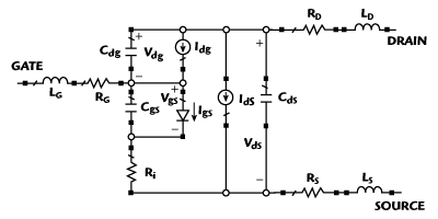 | ||
| Fig. 2 Equivalent circuit of a pulse-doped GaAs MESFET. | ||
Equations for these parameters were developed as functions of Vgs and Vds
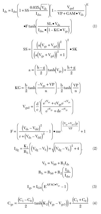
As stated before, pulse-doped devices present a uniform transconductance in nominal operating conditions and a contracted transconductance with a positive gate bias. Equation 1 provides a good analytical expression, both in linear and saturation regions, for the description of the drain current source Ids in the pulse-doped MESFET. Idss is the drain saturation current at zero Vgs, VP represents pinch-off voltage and GAM is the pinch-off slope parameter. SL and SS with fitting parameters h, g, Vgs1 and SK affect the slope of the IV curves in the linear and saturation regions. KG with parameters b and n, and F with parameters r, m, Vds1, Vgs2 and p represent Vgs and Vds dependence in the knee region. Vgsd takes into account the Vgs dependence in the saturation region with c and d as fitting parameters.
The breakdown current Idg is given by the functions listed in Equation 2 with parameters Vb (breakdown voltage) and Rb (series resistance) as dependent variables of Ids.7 Due to the high breakdown voltage of the device (> 25 V) used in testing and modeling for this article, the contribution from the breakdown current was insignificant at the bias voltage (Vd = 4–12 V) of interest. However, for devices with low breakdown voltages, the breakdown current between gate and drain will become significant at large RF swings, modifying the bias conditions and limiting the output power. Equation 2 was derived from work by Tajima, et al.,7 but modified to eliminate the singular point to improve convergence in the calculations.
It is assumed that the gate junction can be approximated by a Schottky barrier diode between the gate and source as a function of Vgs. The gate-to-source current Igs is described in Equation 3 with the model parameters IG0 and AFAC.4 The bias dependency of the intrinsic element Cgs is expressed by the function in Equation 4, with model parameters C1, C0, Vgs3 and K2. The equation provides the variation of Cgs between Vgs (=Vgs–Vgs3 = 0 V) and Cgs when the gate is pinched off. The small dependency of Cgs and Cdg on Vd is not considered significant enough to alter the simulation results of RF output power at the fundamental, second harmonics or intermodulated power levels. However, the Cgs dependency on Vgs was found to significantly affect power saturation and the third-order intermodulation levels.
 | ||
| Fig. 3 ACCO USA Model AU2400 pulsed IV measurement system. | ||
The device used for verification was a Sumitomo GaAs pulse-doped MESFET with 2.8 mm total gate periphery. Each gate finger was 0.3 µm long and 200 mm wide. The pulsed IV characteristics were measured from various quiescent bias points, using the set up shown in Figure 3. Narrow pulses of 0.2 µs were used to take the complete IV characteristics. The data, taken at the bias voltages of Vd = 8 V and Vg = –1.48 V, is shown in Figure 4. Superimposed on these curves are simulated IV curves using Equation 1 as implemented in MWO. Agreement between the two sets of curves (measured and modeled) is excellent. Models at Vd = 4, 8 and 12 V bias points are separately derived and implemented in the ADS and MWO simulators with a user-friendly pull down menu format. An example is shown in Figure 5.
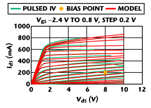 | ||
| Fig. 4 Modeled and measured IV characteristics. | ||
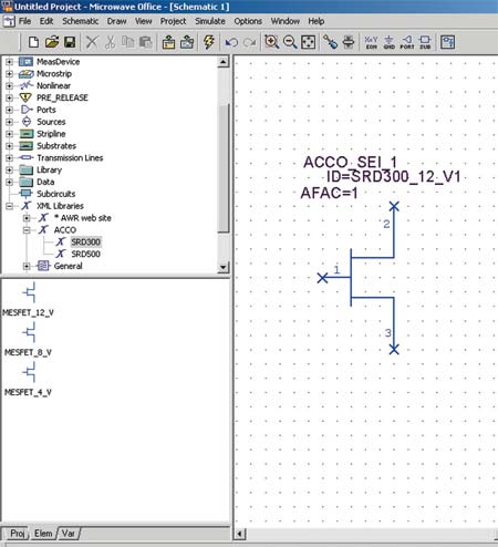 | ||
| Fig. 5 FET models implemented in Microwave Office. | ||
Small-signal extraction methods,8,9,10 using S-parameter data of the device, are used to determine the intrinsic and extrinsic elements. The extrinsic elements Lg, Rg, Ls, Rs, Rd and Ld are bias independent, and the intrinsic elements Cgs, Cdg, Cds and Ri are functions of the biasing conditions. The comparison of the S-parameters is illustrated in Figure 6, which shows reasonable agreement between simulation and measurement.
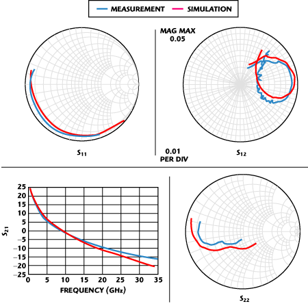 | ||
| Fig. 6 S-parameters measured and simulated at Vd = 8.0 V, Vgs = -1.6 V and F = 0.5 to 35 GHz. | ||
Figure 7 plots the output power, gain and PAE versus input power. The error in output power and gain is within 1 dB, while the PAE is computed with an accuracy better than five percent. Figure 8 shows the output power and the third-order intermodulation product versus input power. The discrepancy of the third-order intermodulation product is approximately 5 dBm.
 | ||
| Fig. 7 Modeled and measured single-tone power data. | ||
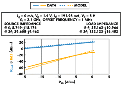 | ||
| Fig. 8 Modeled and measured two-tone power data. | ||
Conclusion
As GaAs MESFET technology continues to advance, large-signal MESFET models are needed to accurately predict performance. The large-signal model, described in this article, has successfully simulated the pulsed IV curves, S-parameters and large-signal RF performance of a pulse-doped GaAs MESFET. The model has been implemented in the industry standard ADS and MWO simulators.
Acknowledgment
This project was sponsored by Sumitomo Electric Industries (SEI).
References
- A. Platzker, A. Palevsky, S. Nash, W. Struble and Y. Tajima, “Characterization of GaAs Devices by a Versatile Pulsed IV Measurement System,” IEEE International Microwave Symposium Digest, 1990, pp. 1137–1140.
- AU2400 from ACCO USA, sales@acco-usa.com, www.acco-usa.com.
- Y. Tajima, B. Wrona and K. Mishima, “GaAs FET Large-signal Model and Its Application to Circuit Designs,” IEEE Transactions on Electron Devices, Vol. 28, No. 2, February 1981, pp. 171–175.
- A. Marterka and T. Kacprzak, “Computer Calculation of Large-signal GaAs FET Amplifier Characteristics,” IEEE Transactions on Microwave Theory and Techniques, Vol. 33, No. 2, February 1985, pp. 129–135.
- W.R. Curtice and M. Ettenberg, “A Nonlinear GaAs FET Model for Use in the Design of Output Circuits for Power Amplifiers,” IEEE Transactions on Microwave Theory and Techniques, Vol. 33, No. 12, December 1985, pp. 1383–1393.
- I. Angelov, H. Zirath and N. Rorsman, “A New Empirical Nonlinear Model for HEMT and MESFET Devices,” IEEE Transactions on Microwave Theory and Techniques, Vol. 40, No. 12, December 1992, pp. 2258–2266.
- Y. Tajima and P.D. Miller, “Design of Broadband Power GaAs FET Amplifiers,” IEEE Transactions on Microwave Theory and Techniques, Vol. 32, No. 3, March 1984, pp. 261–267.
- G. Dambrine, A. Cappy, F. Heriodore and E. Playez, “A New Method for Determining the FET Small-signal Equivalent Circuit,” IEEE Transactions on Microwave Theory and Techniques, Vol. 36, No. 7, July 1988, pp. 1151–1159.
- M. Berroth and R. Bosch, “Broadband Determination of the FET Small-signal Equivalent Circuit,” IEEE Transactions on Microwave Theory and Techniques, Vol. 38, No. 7, July 1990, pp. 891–895.
- S. Lee, H.K. Yu, C.S. Kim, J.G. Koo and K.S. Nam, “A Novel Approach to Extracting Small-signal Model Parameters of Silicon MOSFETs,” IEEE Microwave and Guided Wave Letters, Vol. 7, No. 3, March 1997, pp. 75–77.
Hsiao-Chun (Sophia) Hsu received her BS degree in communication engineering from National Chiao Tung University, Taiwan, in 1995, and her MS degree in electrical and computer engineering from the University of Massachusetts, Amherst, MA, in 2001. From 1995 to 1996, she worked as an RF design engineer at the Computer and Communications Research Laboratories of the Industrial Technology Research Institute, Taiwan. From 1996 to 1998, she worked as a teaching assistant at National Cheng Kung University and National Chiao Tung University, both located in Taiwan. Since 2001, she has been working with ACCO USA, Littleton, MA, focusing on device modeling and RF circuit design.
Yusuke Tajima received his BS and PhD degrees from Tokyo University, Tokyo, Japan, in 1968 and 1980, respectively. From 1968 to 1979, he worked for the Toshiba Corp., Kawasaki, Japan, where he was engaged in the research and development of microwave semiconductor devices and circuit components. In 1979, he joined Raytheon’s Research Division, Waltham, MA, and then transferred to the company’s Microelectronics Division, Andover, MA, where he worked on the design and development of microwave devices, circuits and systems. Since 2000, he has been the general manager of ACCO USA, Littleton, MA, a company specializing in developing analog, RF and microwave integrated circuits and RF test equipment.
