
Having settled on the Cauer-Chebyshev topology, a question arises as to the importance of the order of the elements in the series resonators. If the elements are ideal L’s and C’s, it clearly should not matter. However, considering the parasitics of all the SMT components and the particular problem with SMT capacitors, it is quite possible that the order of elements may have a significant effect.
Experiments were run to determine the effects. In one experiment, the capacitors were placed at the common junction in the center as shown in Figure 9. The result, shown in Figure 10, is a spurious response much closer to the passband edge. This was the result of one experiment and several other layout options can be investigated.

Figure 9 N = 3 Cauer-Chebyshev elliptic function filter with all capacitors at the common junction.

Figure 10 Frequency response of the Figure 9 topology.

It is also interesting to look at the final element values for these two options and compare them to the ideal lumped prototype. This has been done in Table 1. In the preferred case with the inductors at the common junction, the inductors are smaller and the capacitors are larger, which is generally easier to realize. With the capacitors at the common junction, it is just the opposite, the inductors are larger and the capacitors are smaller when compared to the ideal prototype.
APPLICATIONS
The original motivation for this work was a preselector switched filter bank for an advanced handheld transceiver. The filter bank covered 0.9 to 6 GHz with eight equal percentage bandwidth filters. To save space, the shunt arms were folded next to the input/output resonators, which adds a little uncertainty to the measured versus modeled results. Some EM modeling of the right-angle connection to the shunt inductors was implemented. Future SMT 3D FEM models may be able to account for spurious coupling between components.
The filter layout for the lowest frequency channel of the switched filter bank is shown in Figure 11. The analysis to this point has allowed the SMT element values to be continuous. In the final optimization, these values have been set to the closest standard values and the final optimization has been performed on the width and length of the microstrip lines between components. Because of the realities of the design process, a certain amount of skepticism is warranted for any software that claims it can automatically pick standard values and find an equal ripple response in the passband.

Figure 11 Layout of the filter for Channel 1 of the preselector switched filter bank.

Figure 12 Predicted versus measured response of the Channel 1 filters.
Channels 1 and 2 of the preselector switched filter bank had acceptable turn-on performance without tuning. The transmission and reflection characteristics for Channel 1 are shown in Figure 12. The response shows that the stopband spurious prediction is quite good. Starting with Channel 3, small corrections were made to element values on the bench. Channels 7 and 8 necessitated a design spin that moved the inductors farther apart and replaced some of the small-value SMT inductors with printed transmission lines. The performance for the complete set of filters in the eight-channel preselector switched filter bank after tuning and one layout spin is shown in Figure 13.

Figure 13 Performance of the switched filter bank after tuning and one layout spin.

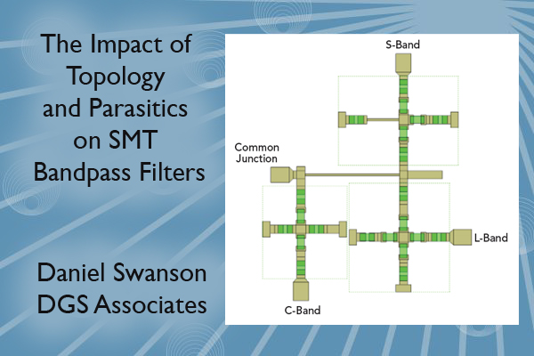
Figure 14 SMT triplexer layout.
Another interesting example is a triplexer designed for Abside Networks6 that covers small segments of the L-, S- and C-Bands. The application is a custom, low-power LTE base station. This design also used the Cauer-Chebyshev filter as the basic building block. The equal ripple optimizer can handle this case just as easily as a single filter and all three channels can be optimized simultaneously during development. The layout for the triplexer is shown in Figure 14. In this design, the shunt inductors for the S-Band and C-Band filters are realized with printed lines and the via inductance.
The simulated performance for the SMT triplexer design is shown in Figure 15 and the measured performance for the circuit is shown in Figure 16. As with the previous example, a small amount of bench tuning was needed to achieve these results. However, a layout spin was not required.

Figure 15 SMT triplexer simulated results.

Figure 16 SMT triplexer measured results after bench tuning.
PCB ETCHED DISTRIBUTED FILTERS
In a multilayer printed circuit board with through vias, the top layer metal is typically about 0.002 in. thick and the tolerance on via placement is no better than +/- 0.003 in. These conditions make it difficult to realize any kind of distributed filter with high accuracy and the filter will also be quite large at lower frequencies. Figure 17 (a)shows the layout for a 3.5 GHz interdigital filter and Figure 17 (b) shows the layout for a 5.8 GHz interdigital filter. Both of these microstrip interdigital filters are fabricated on 0.012 in. thick Rogers 4003 material. The relative size of the filters can be gauged based on the SMA connector footprint. Included in the design and fabrication are photoetched metal covers over each filter.

Figure 17 (a) 3.5 GHz interdigital filter. (b) 5.8 GHz interdigital filter.