
Matching microwave to components within a circuit has become more challenging for the circuit designer as operating frequencies and circuit complexity increase.
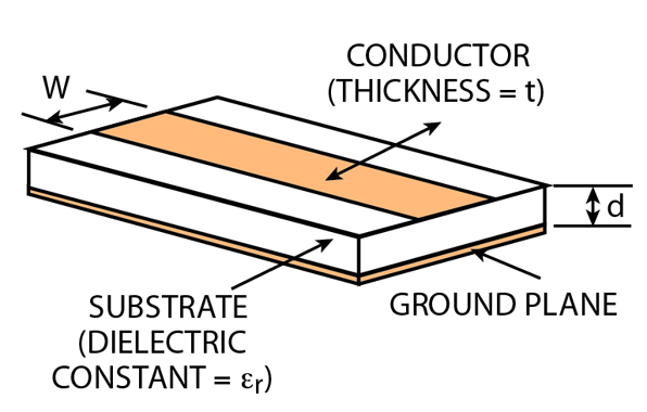
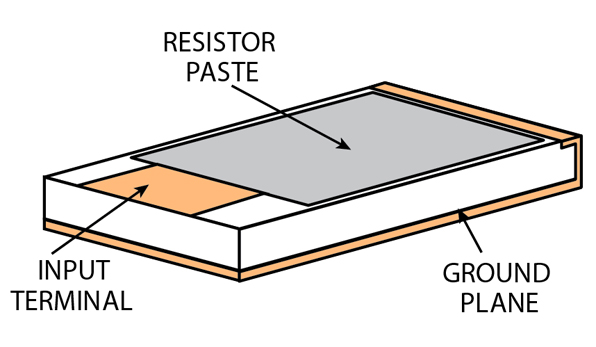
Increasing use of thick film and thin film resistors as 50  terminations has answered the increased need for microwave circuit components in various wireless and telcom applications. This article describes new thick film components designed to aid the circuit designer in efficiently matching the transmission line of a circuit to a chip termination. Primarily, these circuits are designed for 50 , but other possibilities occur at 75 and 100 . The products and methods mentioned here are applicable to any impedance. Figure 1 depicts a section of microstrip transmission line and Figure 2 shows a typical chip termination resistor. As technology advances, so does the need for increased efficiency of energy transmission at elevated frequencies within these systems and components. Optimum energy transmission within the circuit is critically dependent on the efficiency of energy transfer between the transmission lines and the terminations.
The main barrier to maximum efficiency is that most termination resistors possess an RF impedance that is not 50 despite the fact that their DC resistance is 50 . This results in a significant fraction of the energy reflected back into the circuit by the unmatched terminations that present an elevated voltage standing wave ratio (VSWR). This reflection degrades the efficiency of the circuit. When the input terminal configuration of the chip resistor is a significant fraction of a wavelength (more than  /8), the efficiency of energy transfer is degraded further.
One solution is to ensure that the input impedance of the termination resistor is designed to be 50 . Unfortunately, this is not practical. Most substrate thicknesses used in the chip resistor industry have dielectric constants of approximately nine, and require an input metal pad width of 0.025" to 0.040" (0.6 to 1.02 mm). This is very close to the thickness of the substrate itself, thereby inhibiting mechanical stability for small chips. On larger chips (0.250" square or larger), placing a 0.025" or 0.040" wide metal input pad would result in a mechanical connection lacking strength due to the large difference in size between the resistor pad and input pad.
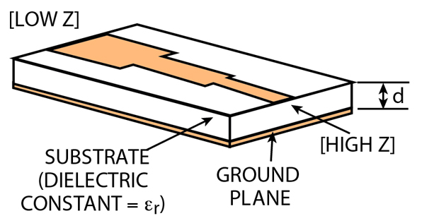
A more viable solution is to place a narrow-band impedance transformer between the incoming transmission line and the termination, as shown in Figure 3 . This device would work well over a limited band of frequencies (typically ±10 percent bandwidth), but the circuit would require an extra component. In addition, the transformer would be larger than the termination itself, thus infringing on valuable circuit board area.
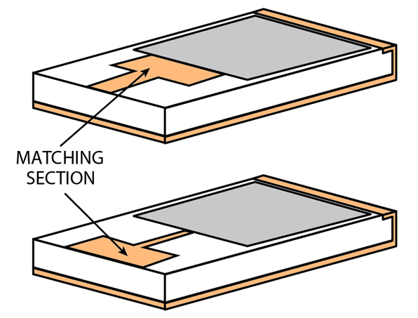
Another solution is provided by IMS' IMT chip termination. This chip termination incorporates an input matching terminal, which eliminates the need for an extra component and simplifies assembly work. Figure 4 shows examples of this device. Essentially, the chip is a 50 absorptive resistor with an L-section placed between the resistor and the incoming transmission line. The L-section is a matching network constructed of lumped element microstrip components and can be designed to match transmission lines of a wide variety of impedances on an individual basis. This provides another means of reducing the VSWR between the transmission line and chip termination. The design of the elements of the matching network depend on the impedance of the incoming transmission line and the size and shape of the terminal to which the transmission line is attached. In addition, this design technique can be applied to terminations with a DC resistance other than 50 .
The bandwidth of this device is necessarily limited. However, an improved VSWR over a 10 percent bandwidth is a typical benefit of using a two-section matched circuit. This product works optimally in circuits where the dielectric constants of the circuit and termination are similar.
Return loss measurements were taken for two different IMS chip terminations. Figure 5 shows typical return loss up to 3 GHz for a chip without a matching section. In this case, the input impedance of the 50 termination (due to the width of the input pad) is approximately 37 . Note that the return loss steadily degrades with increasing frequency (a typical result). This is the result of a host of factors, the most important of which is that the length of the input terminal on the chip approaches a significant fraction of a wavelength as the frequency increases. What cannot be avoided is that the chip looks capacitive to the transmission line, because the impedance of the chip is lower than 50 . This has very little effect at low frequencies but begins to dominate the response as frequency is increased above 1 GHz.
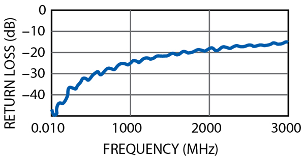
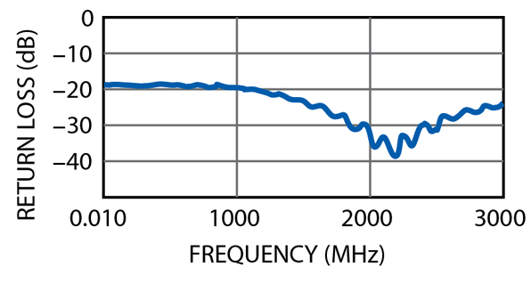
Figure 6 shows typical return loss over the same frequency range of an IMT chip termination with an input matching network. The elements in the L-section were designed to produce a match at approximately 2 GHz. A simple change in the characteristics of the elements would allow for a match at other frequencies where the area of improved VSWR would still represent an approximate 10 percent bandwidth. To achieve a wider bandwidth, more sections would need to be added to the input. Additional sections would significantly reduce the power handling capacity of the chip as more of the substrate area would be dedicated to the matching network than to the resistor itself.
In each case, the incoming transmission line was characterized at 50 and a fixture using a coax (SMA) to microstrip launch was used to test the devices. The microstrip launch was fabricated out of 0.040" thick alumina (Al2O3) and the tested devices were fabricated on 0.040" thick aluminum nitride (AlN). The launch itself was approximately 0.500" in length and the tested devices were each 0.375" in length. The elements in the L-section average approximately 0.060" in length. They function quite well as lumped elements in this example given that a wavelength in microstrip is approximately 1.3" at 3 GHz. This suggests that the chip will function well at 6 GHz also, provided that the elements in the input section are designed accordingly.
This method of input matching can be performed for any frequency band as long as the lengths of the elements are constrained by the previously explained limits. For instance, if a chip termination were designed for 6 GHz, rather than at 2 GHz, the element characteristics would be adjusted so that the performance of the chip was optimized at 6 GHz. Depending on the size of the elements and the overall size of the chip, the adjustment in length may or may not be significant.
Essentially, lumped elements can be practically realized at microwave frequencies provided that their length limitations, as noted previously, are imposed. However, there are many undesirable effects that can mitigate the use of lumped elements in a microwave circuit design if they are not compensated for. A few of these effects are parasitics, fringing effects, resonances and ground plane perturbations, none of which were taken into account in the present analysis.
|
Table 1 | ||
|
|
Standard |
IMT Device |
|
DC resistance ( |
50 |
50 |
|
Dimensions (in) |
0.375 x 0.250 x 0.040 |
0.375 x 0.250 x 0.040 |
|
Power rating |
200 |
170 |
|
VSWR (10% BW) |
1.25 |
1.05 |
The new IMT chip terminations can be fabricated on alumina or aluminum nitride of various thicknesses. AlN will provide good high power terminations as the thermal conductivity of AlN differs from Al2O3 by a factor of about five. If the characteristics of the transmission line are known, most terminations can be effectively matched (with a resulting 10 percent bandwidth) using a two-element method. In this case, the return loss of the device can be improved by 5 to 10 dB. With either substrate material, the high impedance sections should be limited to no more than 100 , which translates to a 0.006" wide trace on a 0.040" thick substrate.
Table 1 lists the specifications for a standard chip termination and the new IMT device. Typical applications for this device include circulators, isolators, directional couplers, 3 dB hybrids and power combiners. Additional information may be obtained via e-mail at ims@ims-resistors.com.
International Manufacturing Services Inc., Portsmouth, RI (401) 683-9700, www.ims-resistors.com. Circle No. 302